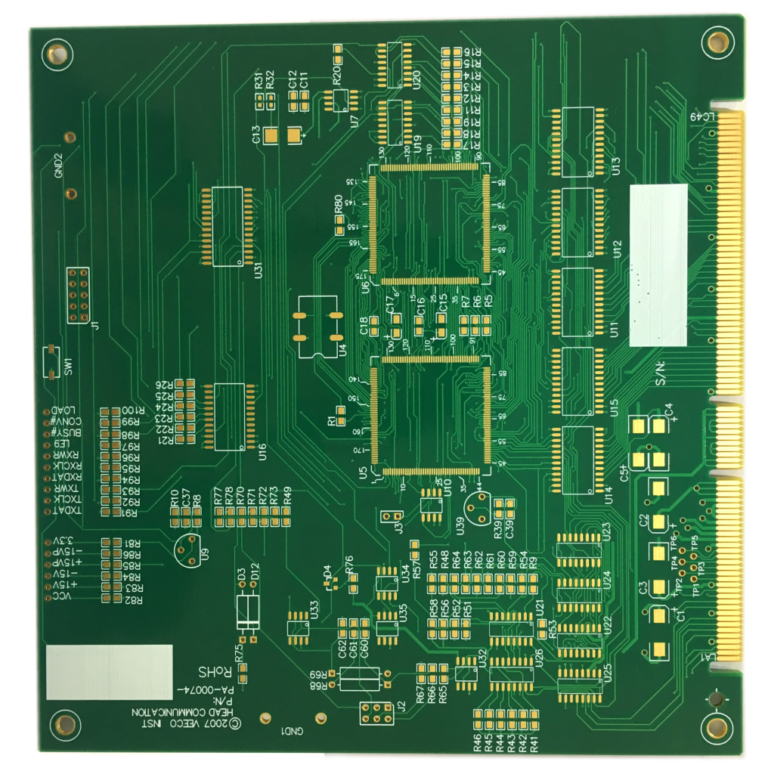
Gold Finger PCB is a circuit board specially designed for connector sockets for connecting other electronic devices or electronic cards. They are typically used in high-density connection applications such as computer motherboards, graphics cards, memory modules, and other devices that require reliable connections.
Related parameters and characteristics:
Connection Areas: The distinguishing feature of a Gold Finger PCB is its connection areas, which are covered with metal, usually gold. These metal connection areas are usually finger-like in shape to ensure a reliable connection.
Material selection: PCB materials are usually selected with higher conductivity and stability to ensure the reliability of metal connections.
Surface Treatment: Gold Finger Metal connection areas on PCBs are typically gold plated to provide excellent electrical performance and corrosion resistance.
Interface type: Gold Finger PCBs can have different interface types, including PCI, PCIe, DIMM, etc., to adapt to different application needs.
Protective measures: Metal connection areas are usually protected to avoid oxidation or contamination and to maintain connection performance.
Size and Shape: Gold Finger PCB sizes and shapes can be customized to meet the needs of specific applications.
If necessary, you can click to view more of our cases.
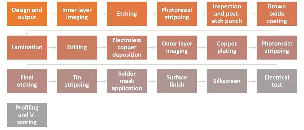
Gold Finger PCB Manufacturing Process:
Design: First, design the circuit board, especially the connection area.
Raw material selection: Choose high-quality fiberglass sheets and metal materials.
Printing: Manufacturing of printed circuits for circuit boards, including the design and fabrication of metal connection areas.
Gold Plating: Metal connection areas are often gold plated to provide good electrical conductivity and corrosion protection.
Assembly: Installing other electronic components and components to complete the circuit board fabrication.
Testing: The Gold Finger PCB is electrically and connectivity tested to ensure its performance and reliability.
Advantages of Gold Finger PCB
✔ Excellent Conductivity: Gold plating provides low electrical resistance.
✔ Superior Durability: High wear resistance for long-lasting performance.
✔ Corrosion Resistance: Gold prevents oxidation and ensures a stable connection.
✔ Reliable Signal Transmission: Ideal for high-frequency applications.
✔ Strong Mechanical Strength: Withstands repeated insertions without degradation.
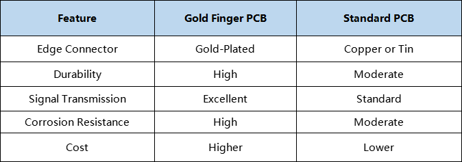
Gold Finger PCB VS. Standard PCB
Our SSD PCB Case
Why Choose Us
Competitive Pricing
More than a decade of experience in the PCB industry ensures quality components at competitive prices.
Fast and reliable delivery
Partnership with multiple global logistics providers ensures timely and reliable shipping.
Quality Assurance
A dedicated quality control team conducts manual visual inspections to ensure all products meet strict quality standards.
We have many international certifications:
We also hold several international quality certifications:
●IATF 16949:2016
●ISO 9001:2015
●ISO 45001:2018
●UL
At the same time, we are always committed to environmental protection. We have an environmental management system certification to ensure that our manufacturing process is environmentally friendly and sustainable.





Frequently Asked Questions(FAQ)
- What gold plating thickness do you offer for Gold Finger PCBs?
We provide 1µm to 50µm gold plating depending on durability and performance requirements.
- Can you manufacture Gold Finger PCBs with custom chamfering?
Yes! We offer customized chamfering angles to optimize insertion performance.
- How can I get a quote for Gold Finger PCBs?
Contact us with your design files, and we will provide a quote within 24 hours.

