
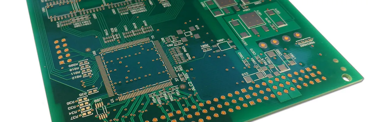
How to improve data transmission speed compared to 4-layer 8-layer SSD PCB?
In the world of data storage, the efficiency and performance of SSDs play a vital role in meeting the demands of modern applications. One of the critical factors that influences SSD performance is its printed circuit board. Specifically, the number of layers in a PCB design can significantly affect data transfer speeds. In this blog post, we will explore how an 8-layer SSD PCB can improve data transfer speeds compared to a 4-layer PCB.
Enhanced Signal Integrity with 8-layer SSD PCB
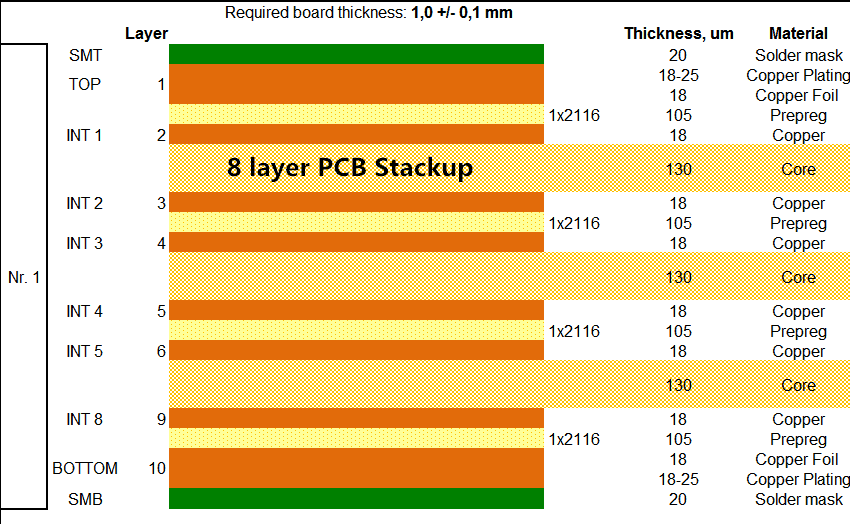
Signal integrity is a crucial aspect of data transfer speeds in SSDs. 8-layer SSD PCBs improve signal integrity by providing additional signal routing layers and ground planes compared to 4-layer PCBs. These extra layers help reduce signal interference and crosstalk, which can degrade performance. 8-layer SSD PCBs have dedicated power and ground planes to minimize noise that can affect data transfer quality. This enhanced signal integrity ensures that data is transferred more reliably at higher speeds, making it an ideal choice for applications that require fast and accurate data access.

Optimized Power Distribution with an 8-layer SSD PCB
Power distribution is another area where 8-layer SSD PCBs outperform 4-layer PCBs. The additional layers in an 8-layer PCB distribute power more efficiently across the board. This provides a more stable voltage supply to SSD components, which is critical for maintaining consistent performance. Stable power distribution reduces the likelihood of voltage drops and fluctuations that can affect data transfer speeds. By ensuring that each component receives a stable and reliable power supply, 8-layer SSD PCBs improve overall performance and data transfer efficiency.
Can Improve Routing Complexity and Efficiency
Compared to 4-layer PCBs, 8-layer SSD PCBs offer greater routing flexibility. Additional layers provide more data signal routing paths, allowing for more complex and efficient signal routing designs. This enhanced routing capability shortens the distance signals need to travel and minimizes potential delays. Additionally, it separates high-speed data lines from low-speed or power lines, further reducing signal interference. As a result, 8-layer SSD PCBs enable faster data transfer speeds and higher overall performance.
Reduce Parasitic Capacitance with 8-layer SSD PCB.
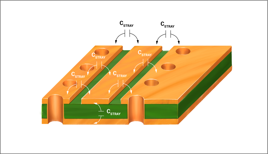
Parasitic capacitance is caused by unwanted capacitance between traces and can adversely affect data transfer speeds. 8-layer SSD PCBs help mitigate parasitic capacitance more effectively than 4-layer PCBs. The extra layers provide better separation between signal traces and power planes, reducing the impact of parasitic effects. The reduction in parasitic capacitance speeds up signal transitions and increases data transfer rates. For users who require high-speed data access, the reduced parasitic capacitance of 8-layer SSD PCBs is a significant advantage.
Improved Thermal Management Prevents Thermal Throttling
Thermal management is critical to maintaining the optimal performance of SSDs. 8-layer SSD PCBs enhance thermal management by providing a larger surface area for heat dissipation and better heat distribution. The extra layers allow for the integration of thermal vias and heat sinks, which helps dissipate heat more effectively. By managing heat more effectively, 8-layer SSD PCBs prevent thermal throttling, which would otherwise reduce data transfer speeds. This improved thermal management ensures that the SSD operates at peak performance, even under heavy loads.
Improved Component Density and Integration
Compared to 4-layer PCBs, 8-layer SSD PCBs support higher component density. The increased number of layers allows for the integration of more components, such as memory chips and controllers, without compromising performance. This higher component density can lead to more advanced SSD designs with greater storage capacity and faster data access times. For industries that require rapid processing of large amounts of data, such as video editing or scientific research, the increased component density of 8-layer SSD PCBs provides significant performance advantages.
More Flexibility in Implementing High-Speed Data Interfaces
Finally, 8-layer SSD PCBs offer greater flexibility when implementing high-speed data interfaces. The additional layers provide more options for high-speed data line routing and integrating advanced interfaces or NVMe. This flexibility enables SSDs to support higher data transfer speeds and bandwidth, making them suitable for demanding applications that require fast data access and processing. By leveraging the advanced capabilities of 8-layer SSD PCBs, users can achieve superior performance in their data storage solutions.
An 8-layer SSD PCB is better than a 4-layer PCB
An 8-layer SSD PCB has several advantages over a 4-layer PCB when it comes to increasing data transfer speeds. Enhanced signal integrity, optimized power distribution, increased routing efficiency, reduced parasitic capacitance, improved thermal management, higher component density, and greater high-speed interface flexibility all contribute to superior performance. By choosing an 8-layer SSD PCB, users can ensure that their data storage systems operate at peak efficiency, providing faster and more reliable access to critical data.