
Are 4 layer gold finger PCB Compatible with Next-Generation 6G Technology?
Demand for high-performance PCBs has surged as the world races to adopt 6G technology. These circuit boards form the backbone of electronic devices, enabling seamless data transfer at increasingly faster speeds. 4 layer gold finger PCBs are prized for their high connectivity, reliability, and durability. In this blog post, we’ll explore the compatibility of 4 layer gold finger PCB with 6G and why they’re essential for the next wave of technological innovation.
Understanding 6G: The Next Step in Wireless Evolution
6G technology represents the next major milestone in wireless communications, with speeds expected to be 100 times faster than 5G. It promises lower latency, increased bandwidth, and improved device connectivity. These advances also pose new challenges for infrastructure, including the printed circuit boards in high-performance networks. In 6G, PCBs must manage ultra-high frequencies and large data volumes efficiently with minimal interference. That’s where 4 layer gold finger PCB comes into play, providing the high-speed interconnects and durability needed to support future telecommunications.
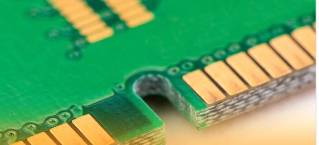
Why 4 layer gold finger PCBs Stand Out?
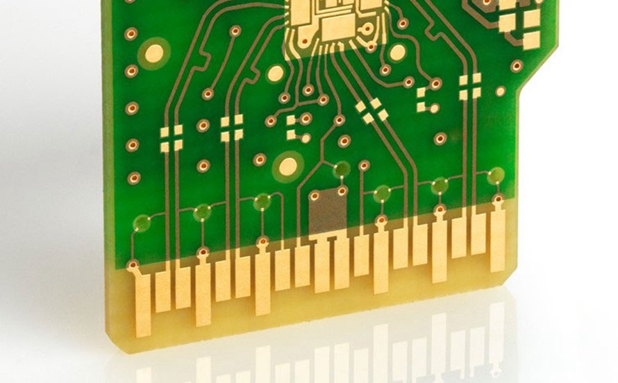
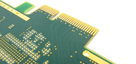
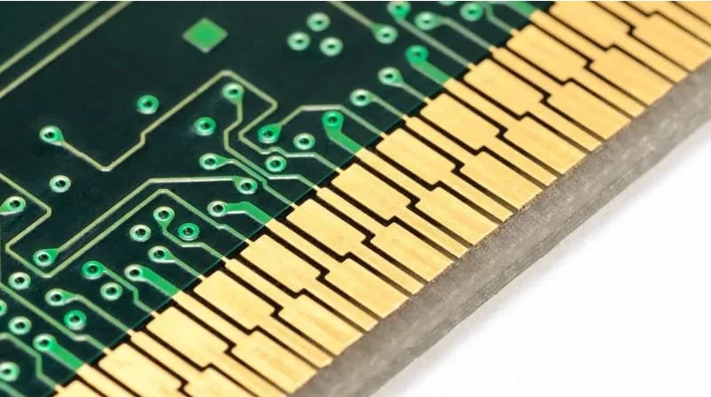
Engineers prefer 4 layer gold finger PCB for their precision, durability, and ability to handle high-speed signals, making them ideal for cutting-edge applications. But why do these PCBs stand out in 6G? The answer lies in their layered structure and gold-plated connectors. With four conductive layers, these PCBs provide design flexibility and signal integrity needed for 6G speeds. Gold fingers ensure excellent conductivity and wear resistance, making these PCBs reliable and durable. In the high-frequency 6G environment, data transmission needs to be smooth and uninterrupted, and these qualities are essential.
How 4 layer gold finger PCBs Handle High Frequency?
A key aspect of 6G technology is that it uses higher frequency bands, typically in the millimeter wave spectrum. Traditional PCBs can have difficulty handling these frequencies or cause severe signal loss or interference. Designers focus on enhanced performance when creating 4 layer gold finger PCB. The additional layers in the PCB allow for more complex routing, which reduces signal loss and improves the overall integrity of the transmitted data. Gold fingers also ensure that connection points remain stable and corrosion-free, minimizing potential disruptions in high-frequency applications. This makes them highly compatible with 6G, which requires robust and efficient signal processing across multiple frequencies.
Durability and Reliability in Harsh Environments
As 6G technology is integrated into various industries, from telecommunications to autonomous vehicles and smart cities, the PCBs that support these networks must withstand multiple environmental conditions. Whether exposed to extreme temperatures, humidity, or physical wear and tear, 4 layer gold finger PCB are durable. The gold plating on the connectors is highly resistant to oxidation and corrosion, ensuring a long service life even in harsh conditions. In addition, the multi-layer structure improves thermal management, which is critical to maintaining performance in high-speed applications. This durability makes 4 layer gold finger PCB compatible with 6G technology and a reliable choice for future-proof infrastructure.
Scalability and Flexibility in Design
4 layer gold finger PCBs offer scalability and design flexibility, crucial for advancing 6G technology. As we move toward more complex electronic devices that require higher bandwidth and faster processing speeds, the ability to customize PCBs to meet specific needs becomes increasingly important. Compared to single- or double-layer PCBs, 4-layer PCBs offer greater design flexibility, allowing engineers to optimize layouts for better signal transmission and reduced interference. Gold fingers ensure reliable, high-speed connections between PCBs and components, ideal for next-gen 6G networks.
The Role of Gold Finger PCBs in the Internet of Things
As 6G technology accelerates the development of the Internet of Things, the need for high-performance PCBs becomes even more critical. 4 layer gold finger PCBs enable fast data transfer and seamless connectivity, which Internet of Things devices rely on. These PCBs ensure quick and efficient data transfer by allowing reliable device communication. In a 6G IoT ecosystem with billions of devices, Gold Finger PCBs will deliver essential high-speed connectivity. Whether used for smart homes, industrial automation, or connected cars, these PCBs will be at the heart of the Internet of Things revolution, supporting the next generation of wireless communications.
The Importance of Investing in 4 layer gold finger PCBs
Looking ahead, it is clear that 4 layer gold finger PCBs will be an integral part of the infrastructure that supports 6G technology. Their ability to handle high frequencies, provide reliable connections, and withstand harsh conditions are ideally suited to the needs of next-generation networks. For businesses and engineers preparing to design and implement 6G systems, investing in high-quality 4 layer gold finger PCBs is critical. These PCBs will ensure the smooth operation of 6G networks and lay the foundation for future innovations in telecommunications, the Internet of Things, and other fields.
4 layer gold finger PCBs for 6G Technology
In conclusion, 4 layer gold finger PCBs are not only compatible with next-generation 6G technology but are also a key component in ensuring the success of these networks. Their unique performance, including high-speed signal processing, durability, and design flexibility, make them well-suited to the challenges of 6G. As industries worldwide prepare for the launch of 6G, it is important to invest in high-quality PCBs.