
How does Heavy Copper PCB Manufacturing differ from Standard PCB Manufacturing?
There is a distinct difference between standard PCB manufacturing and Heavy Copper PCB manufacturing in printed circuit boards. Heavy copper PCBs are circuit boards that handle higher current loads and extreme environmental conditions. Their unique structure makes them ideal for demanding applications such as industrial controls, power converters, and electric vehicles. This blog post will explore the differences between Heavy Copper PCB manufacturing and standard PCB production.
Differences in Heavy Copper PCB Manufacturing
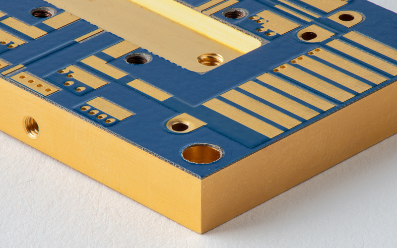
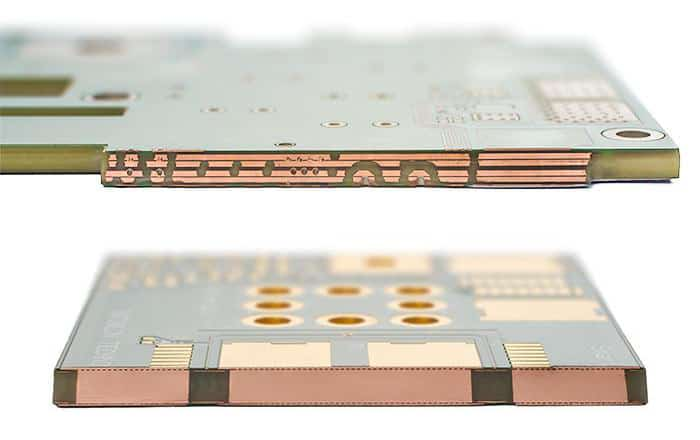
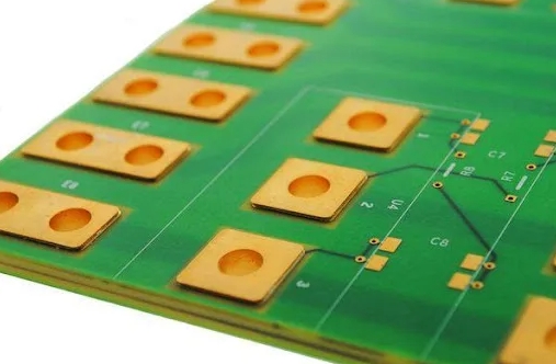
Heavy copper PCB manufacturing produces boards with significantly thicker copper layers than standard PCBs. While standard PCBs typically use copper layers between 1 oz/sq. Ft. and 3 oz/sq. Heavy copper PCBs can have copper layers of 4 oz/sq. ft. copper layers or more, with some designs exceeding 20 oz/sq. Ft. Increasing copper thickness enables heavy copper PCBs to carry higher currents and dissipate heat more effectively, making them suitable for power electronics and industrial applications.
The core difference lies in the manufacturing process. It requires specialized equipment and techniques because thicker copper layers must be precisely plated and etched. Traditional methods used for standard PCBs have difficulty handling such high copper volumes, leading to challenges in layer adhesion, trace width control, and via formation.
A Detailed Introduction to Manufacturing Technologies
The technologies used in heavy copper PCB manufacturing are more complex and intricate than those used in standard PCB manufacturing. While the beginning of the process is similar, involving the deposition of a copper layer onto a substrate, additional steps are required to ensure the integrity and functionality of the heavier copper layer.
Manufacturers often employ advanced techniques, such as step or differential plating, for heavy copper PCB manufacturing. These processes enable manufacturers to build thicker copper layers in specific PCB areas requiring high current loads or thermal management. Additionally, enhanced etching methods are needed to maintain the integrity of the circuit paths without compromising surrounding materials. In contrast, standard PCBs rely on simpler etching and lamination processes due to their thinner copper layers.
Manufacturing Material Considerations
The materials used in heavy copper PCB manufacturing differ from those used in standard PCB construction. The need to manage higher thermal loads, withstand mechanical stress, and ensure long-term reliability drives the selection of specialized substrates, resins, and prepregs.
Manufacturers typically use reinforced fiberglass substrates with high thermal conductivity in heavy copper PCB manufacturing to better dissipate the heat generated by thicker copper layers. Advanced resin systems are also selected because they resist expansion and contraction under temperature changes, a critical property in high-power applications. In contrast, standard PCBs typically use FR4, a joint fiberglass epoxy laminate material that may not provide the same durability or heat resistance required for heavy copper designs.
Cost and Production Time Comparison
One of the main differences between heavy copper PCB manufacturing and standard PCB production is the cost and production time involved. Thick copper PCBs are inherently more expensive due to the specialized materials, equipment, and processes required. The plating technology used and the precision of The additional stresses created during etching and drilling add to the complexity and duration of the manufacturing process.
Production time is relatively short in standard PCB manufacturing due to the streamlined processes involved. The copper layers are thinner, and the equipment used to etch and plate these layers can operate efficiently in a shorter time. In contrast, heavy copper PCB requires more time for plating and etching because the thicker copper layers require longer exposure times in each step.
More suitable for high-power applications
Manufacturers design heavy copper PCBs to excel in high-power, high-temperature environments where standard PCBs would fail. Thicker copper layers can increase current-carrying capacity, critical for applications involving power conversion, motor control, and other industrial functions. This higher capacity ensures the PCB can safely handle electrical loads without overheating or damaging components.
In addition to increased current handling capabilities, it also provides superior thermal performance. Thicker copper layers act as influential thermal conductors, dissipating heat more efficiently and reducing the risk of hot spots that can cause component failure. Standard PCBs have thinner copper layers that are more susceptible to heat buildup and may require additional cooling mechanisms to maintain safe operating temperatures.
Areas where Heavy Copper PCB Manufacturing is Indispensable
Various industries use heavy copper PCB manufacturing where reliability, performance, and durability are critical. For example, the automotive industry relies on heavy copper PCBs in electric vehicles for power distribution and control systems. These boards ensure that the electrical systems in electric cars can handle the high current loads required for efficient performance, especially in battery management and charging systems.
Heavy copper PCBs are vital in power converters, inverters, and motor controllers in industrial control and power electronics. Their ability to manage high current and voltage levels without compromising performance or safety makes them a preferred solution for such applications. Similarly, renewable energy systems, especially solar and wind converters, benefit from heavy copper PCBs’ superior current-carrying capacity and heat dissipation capabilities.
More stringent quality control and testing
The quality control and testing processes for heavy copper PCB manufacturing are more stringent than those for standard PCB production. Given the critical applications of heavy copper PCBs, manufacturers must ensure that each board meets strict performance, reliability, and safety standards. Testing procedures such as thermal cycling, high current, and mechanical stress testing are standard practices for heavy copper PCB manufacturing.
In addition, the plating and etching processes must be carefully monitored to prevent defects such as voids, delamination, or improper trace formation. Thicker copper layers require more precise control of these processes to ensure that the final product meets the required specifications. While subject to quality control, standard PCBs are not subject to the same level of scrutiny as heavy copper boards because the performance requirements are lower.
Heavy Copper PCB Manufacturing for High-Power Applications
Heavy Copper PCB manufacturing offers advantages over standard PCB production, especially in high-power and high-temperature applications. Using thicker copper layers, advanced manufacturing techniques, and specialized materials ensures these boards can handle greater electrical loads and dissipate heat more effectively. While Heavy Copper PCBs’ cost and production time may be higher, the long-term advantages in reliability, durability, and performance make them a valuable investment in industries such as automotive, industrial controls, and renewable energy.