
What is the maximum current-carrying capacity of a 2 layer HAL PCB?
When choosing a 2 layer HAL PCB for your electronic application, it is crucial to understand its maximum current-carrying capacity. This capacity determines how much current the PCB can handle without overheating, which affects performance and reliability. The following blog post will explore this critical factor, focusing on how different design elements, such as copper thickness, trace width, and thermal management, affect the maximum current-carrying capacity of a 2 layer HAL PCB.
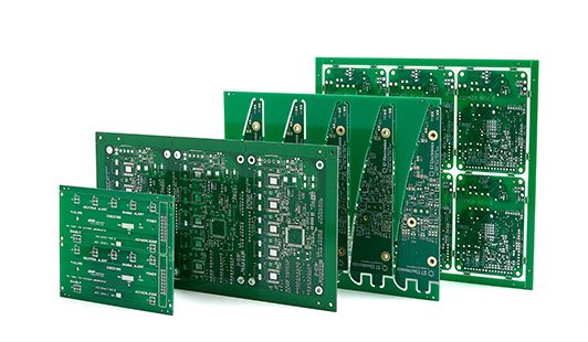
Understanding 2 layer HAL PCB and Their Construction
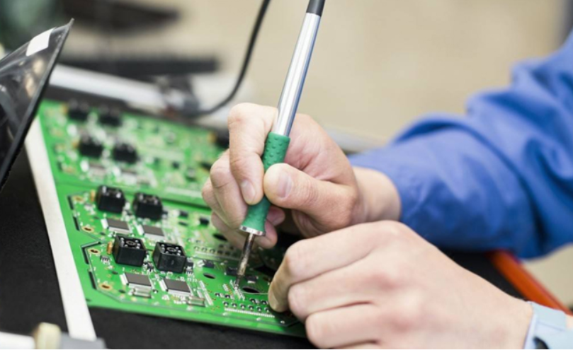
Before discussing the maximum current-carrying capacity of 2 layer HAL PCBs, it is crucial to understand how they differ from other types. 2 layer PCBs have two layers of conductive copper with a dielectric layer in between. HAL is a finishing process that applies molten solder to the exposed copper pads of the board and then flattens it with hot air to create a smooth surface. This ensures that the solder joints are robust, reliable, and long-lasting.
The HAL coating also adds a protective layer to prevent oxidation, helping to improve conductivity over time. While 2 layer HAL PCBs are popular in various electronic applications, their performance in high-current environments depends mainly on the board’s design, including copper thickness and layout. Factors such as trace width, copper weight, and operating environment affect the board’s ability to carry current without overheating or suffering electrical performance degradation effectively.
How Copper Thickness Affects Its Maximum Current-Carrying Capacity
Copper thickness is one of the most critical factors in determining the current-carrying capacity of a 2 layer HAL PCB. Generally speaking, the thicker the copper, the more current it can carry without generating excessive heat. Most PCBs have a standard copper thickness of 1 oz/ft2 (about 35 microns), but for high-current applications, manufacturers may choose thicker copper layers, such as 2 oz/ft2 or even 3 oz/ft2.
For 2 layer HAL PCBs, current-carrying capacity increases proportionately to copper thickness because thicker copper traces offer less resistance to the current flow. This reduced resistance means lower heat generation, critical to maintaining the board’s life and performance. For example, a 1 oz/sq ft copper trace can handle about ten amps, while a 2 oz/sq ft trace can carry almost twice as much.
Trace Width and Its Effect on Its Current Carrying Capacity
In addition to copper thickness, the width of a trace on a 2 layer HAL PCB can significantly affect its maximum current-carrying capacity. Trace width determines the current’s space to flow through, and wider traces can carry more current with less resistance. According to the IPC-2221 standard, the relationship between trace width, copper thickness, and allowed current is clear.
For example, a trace with a width of 0.5 mm and a copper layer thickness of 1 oz/sq ft might carry about ten amps, while increasing the width to 1 mm might double the current. The formula used to calculate the maximum current carrying capacity of a PCB trace is based on the cross-sectional area of the trace, and the allowed temperature rise. When current flows through a trace, heat is generated; if the heat is not dissipated correctly, it can damage the PCB and reduce the reliability of the electronic components. Designers must carefully calculate the appropriate trace width for their 2 layer HAL PCB based on the expected current load and environmental conditions.
Thermal Management and Its Role in Maximum Current Carrying Capability
Thermal management is a critical consideration in determining the maximum current carrying capacity of a 2 layer HAL PCB. When current flows through copper traces, it generates heat due to resistance. If this heat is not managed correctly, it can raise the board’s temperature, potentially damaging components or shortening the PCB’s life.
In high-power applications, designers can also incorporate heat sinks or thermal vias to help dissipate heat. Heat sinks can be attached to high-current areas of the PCB to draw heat away from traces, while thermal vias can provide a path for heat to escape through the board layers. By effectively managing heat, designers can increase the maximum current-carrying capacity of a 2 layer HAL PCB, ensuring it can operate reliably even under harsh conditions.
Effect of Solder Mask and Surface Finish on Maximum Current-Carrying Capacity of 2 layer HAL PCB
The surface finish of a PCB, especially that of a 2 layer HAL PCB, plays a vital role in its performance. The HAL process coats copper pads with a thin solder layer, which helps prevent copper oxidation and ensures a reliable connection between components and the board. While the primary purpose of the solder mask and surface finish is to improve solderability, they can also indirectly affect the board’s thermal and electrical performance.
A smooth, uniform HAL surface finish provides a uniform surface for solder joints, preventing localized hot spots and helping to dissipate heat better. Additionally, HAL surface finishes can help protect the board from environmental factors such as moisture or contaminants that can degrade the PCB’s performance over time.

Environmental Factors and Their Impact on Maximum Current-Carrying Capacity
The operating environment of a 2 layer HAL PCB can also affect its maximum current-carrying capacity. Ambient temperature, airflow, and humidity can affect the board’s ability to dissipate heat and handle electrical loads. For example, in high-temperature environments, a PCB may require wider traces or thicker copper layers to compensate for reduced heat dissipation. Similarly, environments with poor airflow can cause heat to build up, limiting the board’s current-carrying capacity.
Humidity and moisture can also affect the performance of a 2 layer HAL PCB because they can cause copper traces to oxidize or corrode. This increases the trace’s resistance, reducing its ability to carry current effectively. To mitigate these risks, PCBs designed for harsh environments often incorporate additional protective coatings, such as conformal or encapsulation, to protect the board from moisture and contaminants.
Design Optimization for Maximum Current-Carrying Capacity
An effective strategy for optimizing the 2 layer HAL PCB design is to use a combination of wider traces and thicker copper layers in areas where high current is expected. Additionally, incorporating thermal vias and heat sinks can help dissipate heat more effectively, preventing hot spots and ensuring even temperature distribution across the board.
Another consideration is the placement of components on the PCB. By placing high-power components away from sensitive board areas, designers can reduce the risk of thermal damage and ensure that the PCB can handle the required current load without issue. Finally, careful attention to the HAL process and the application of protective coatings can enhance the durability and reliability of the PCB, ensuring it performs optimally in high-current environments.
Maximizing the Current-Carrying Capacity of a 2 layer HAL PCB
The maximum current-carrying capacity of a 2 layer HAL PCB depends on several critical factors, including copper thickness, trace width, thermal management, and environmental conditions. By optimizing these elements, designers can create PCBs that meet the current requirements of their applications and provide reliable, long-lasting performance.