
Effect of copper thickness on 4 Layer Heavy Copper PCB signal
In the world of printed circuit boards, the configuration and materials used can significantly impact performance. Designed to handle high current loads and provide excellent signal integrity, the 4 layer heavy copper PCB has a copper thickness, which is a critical aspect that directly impacts signal integrity. This blog post will explore how copper thickness affects signal integrity in 4 layer heavy copper PCBs.
Understanding 4 Layer Heavy Copper PCBs
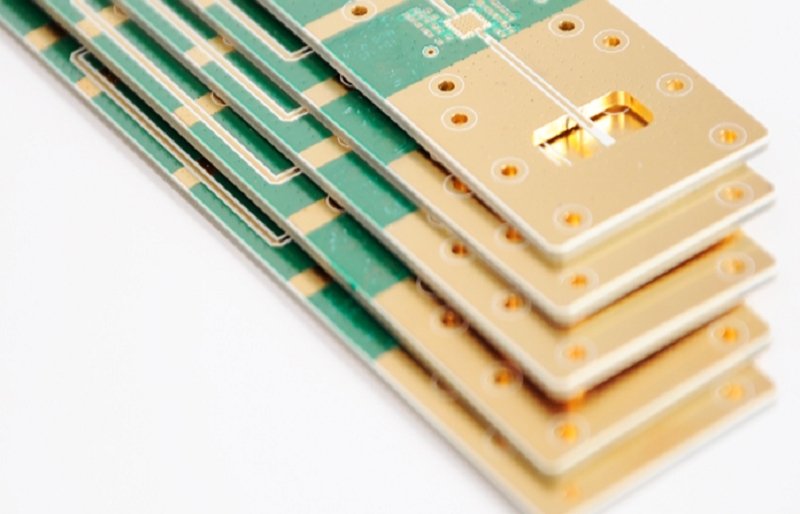
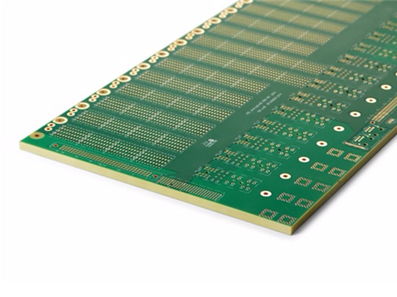
A 4 layer heavy copper PCB typically consists of four conductive layers and is designed to handle high current densities. Unlike standard PCBs, which may utilize lighter copper, heavy copper PCBs feature copper thicknesses ranging from 4 oz/ft² to 20 oz/ft² or more. The increased copper thickness provides enhanced conductivity, allowing for higher current-carrying capacities without overheating or signal degradation.
A 4 layer heavy copper PCB usually consists of two outer layers for signal transmission and two inner layers used primarily for power distribution and ground connections. This structure is particularly advantageous in applications such as power supplies, automotive systems, and industrial equipment, where reliability and performance are paramount. Understanding the importance of copper thickness in these applications can help users make informed decisions when purchasing these specialized PCBs.
The Role of Copper Thickness in Signal Integrity
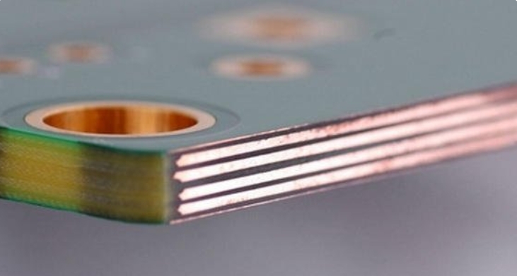
Copper thickness plays a pivotal role in determining the signal integrity of a 4 layer heavy copper PCB. Signal integrity refers to the quality of an electrical signal as it travels through a conductor, influenced by factors such as attenuation, noise, and distortion. A thicker copper layer helps reduce the resistance of the traces, enabling a more reliable flow of electrical signals.
When signals travel through a PCB, they experience resistance, which can lead to signal loss or distortion. Increasing the copper thickness minimizes resistance, which can improve signal quality and accelerate data transfer rates.
How Copper Thickness Affects Impedance Control
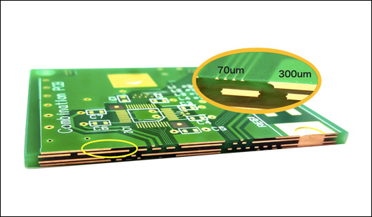
Another critical factor related to signal integrity in 4 layer heavy copper PCBs is impedance control. Impedance measures the opposition a circuit presents to a current when voltage is applied. The PCB’s design, including the copper thickness, dielectric material, and trace geometry, directly influences impedance characteristics.
With heavier copper layers, the impedance of the traces can be controlled more effectively. This is crucial in high-speed digital circuits, where maintaining a consistent impedance helps prevent signal reflections that can degrade performance. Inadequate impedance control can result in signal integrity issues, leading to data errors and reduced reliability. By optimizing copper thickness in conjunction with other design parameters, manufacturers can enhance the overall performance of the PCB.
Impact of Copper Thickness on Heat Dissipation
The increased copper thickness in a 4 layer heavy copper PCB improves signal integrity and thermal management. Higher current loads generate heat, and effective heat dissipation is crucial for maintaining performance and preventing component failure. Thicker copper layers can absorb and distribute heat more efficiently, reducing the risk of hot spots that can negatively impact signal integrity.
Moreover, better thermal performance allows components to operate within their optimal temperature ranges, further contributing to signal integrity. In high-frequency applications, excessive heat can lead to increased resistance and subsequent signal loss. By investing in 4 layer heavy copper PCBs with appropriate copper thickness, users can ensure that their designs maintain signal integrity even under demanding thermal conditions.
Minimizing Electromagnetic Interference with Copper Thickness
Electromagnetic interference is another concern that can affect signal integrity in PCBs. Thicker copper layers can help reduce susceptibility to EMI by providing better shielding for the signals transmitted across the board. EMI can induce unwanted signals or noise that interferes with the proper operation of electronic devices, leading to degraded performance.
In a four-layer heavy copper PCB, the additional copper thickness acts as a barrier against external electromagnetic fields, enhancing the board’s overall resilience to interference. Furthermore, proper grounding and power distribution layers, in conjunction with thicker copper, can help minimize ground loops, a common source of noise in electronic systems. By ensuring that the PCB design incorporates adequate copper thickness, manufacturers can significantly improve the signal integrity and reliability of their products.
Design Considerations for Optimizing Copper Thickness
When designing a 4 layer heavy copper PCB, several factors should be considered to optimize copper thickness for signal integrity. These factors include the intended application, frequency of operation, and current requirements. Understanding the specific needs of the application will guide the decision-making process regarding copper thickness.
For instance, high-frequency applications may benefit from thinner copper layers to reduce capacitance and improve signal rise times. In contrast, low-frequency or high-power applications may require thicker copper to manage current loads effectively. Engineers and designers must collaborate closely with PCB manufacturers to determine the optimal copper thickness that aligns with their project requirements, ensuring a successful outcome.
Future Trends in 4 layer Heavy Copper PCB Technology
As technology continues to advance, the demand for higher-performance and more reliable 4 layer heavy copper PCBs is expected to grow. Emerging applications such as electric vehicles, renewable energy systems, and advanced communication technologies require PCBs that can handle increased current loads while maintaining excellent signal integrity.
Manufacturers are increasingly focusing on innovations that enhance copper thickness management and overall PCB performance. This includes advanced materials and fabrication techniques that improve thermal performance and EMI shielding capabilities. Users looking to invest in 4 layer heavy copper PCBs should stay informed about these trends to ensure they choose the most effective solutions for their applications.
Copper thickness is critical for 4 layer Heavy Copper PCB signal integrity
As technology evolves, optimizing copper thickness in PCB design will continue to play a crucial role in enhancing performance and reliability in various applications. By understanding the relationship between copper thickness, signal quality, impedance control, thermal management, and EMI shielding, users can make informed decisions when purchasing these essential components.