

How does solder mask application differ for a 2 layer HAL PCB?
When designing a printed circuit board, an important aspect that should not be overlooked is the application of a solder mask, especially in 2 layer HAL PCB. A solder mask is a protective layer applied to the surface of a PCB that serves a variety of purposes. It acts as a barrier to environmental pollutants, prevents solder bridging during assembly, and contributes to the overall aesthetics of the PCB. The differences in the solder mask application process in 2 layer HAL PCB can significantly affect the quality and functionality of the final product.
The Importance of Solder Mask in 2 Layer HAL PCB
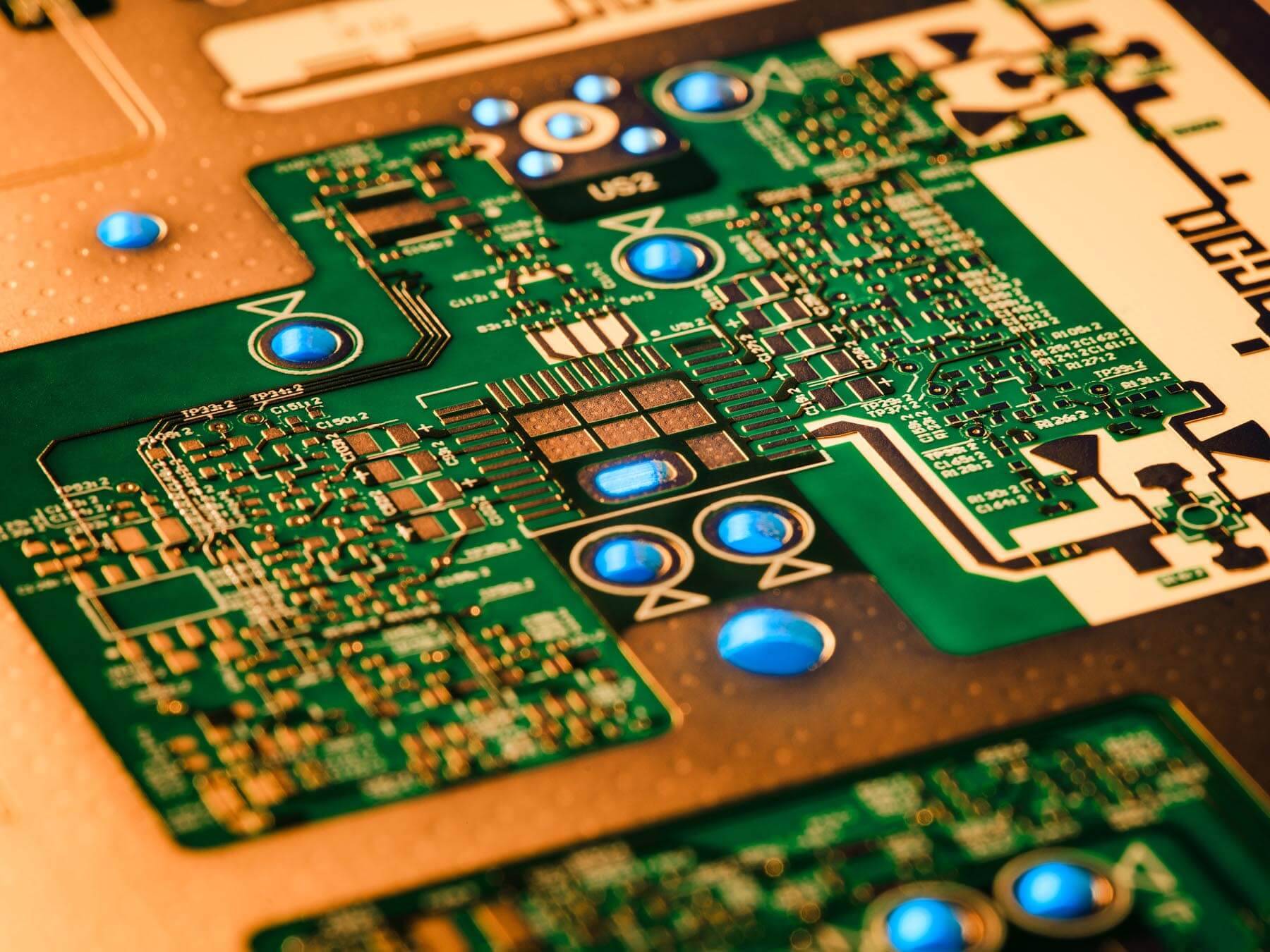
The solder mask serves a pivotal role in the performance and reliability of a 2 layer HAL PCB. By providing a protective layer, it prevents oxidation of copper traces, which is vital for maintaining electrical conductivity. This is particularly important in environments that are prone to moisture or other corrosive elements. Furthermore, the solder mask enhances the mechanical integrity of the PCB by adding a layer of protection against physical stressors. In the manufacturing process of a 2 layer HAL PCB, any failure to adequately apply the solder mask can lead to various issues, including short circuits, component failures, or even total board failure.
In addition to protection, the solder mask also plays a crucial role in ensuring the manufacturability of the PCB. During assembly, the solder mask prevents solder from flowing onto unwanted areas, reducing the risk of solder bridges—unintended connections between two or more pads. This is particularly significant in a 2 layer HAL PCB, where multiple components are placed in close proximity. Proper solder mask application ensures a controlled and accurate soldering process, minimizing the likelihood of defects caused by improper solder placement. As a result, the overall yield and quality of the 2 layer HAL PCB improve.
Solder Mask Types and Their Applications
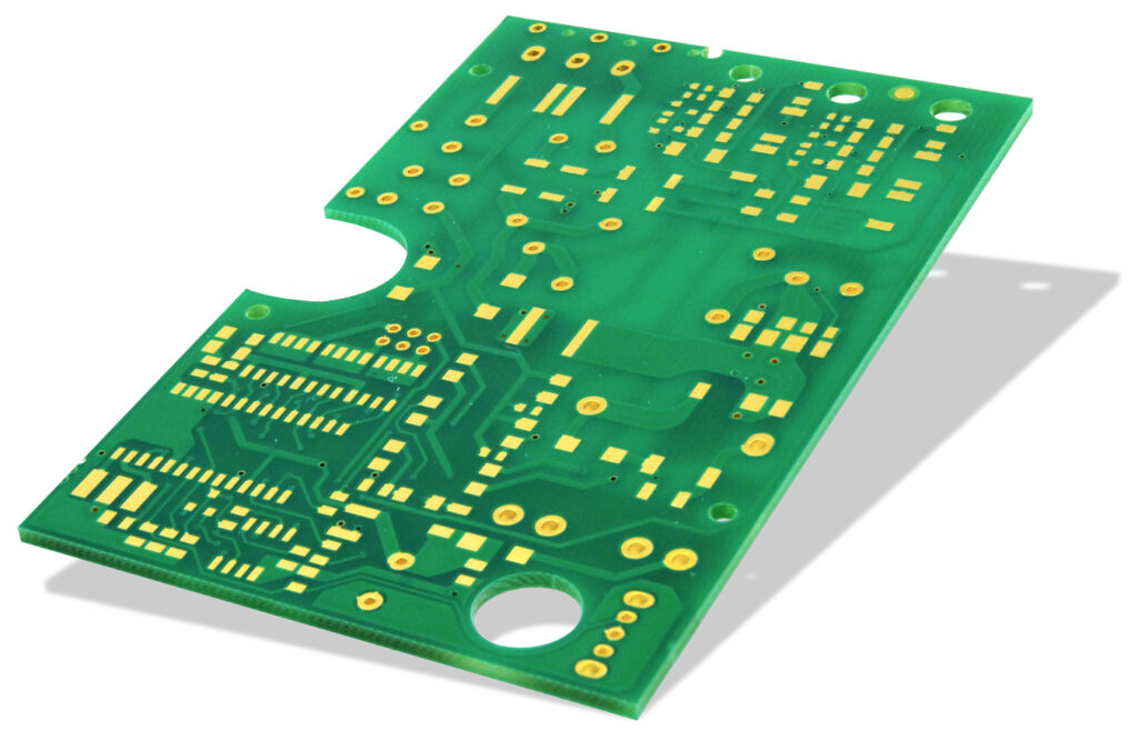
Manufacturers can employ various types of solder masks in the production of 2 layer HAL PCBs, each offering distinct advantages depending on the application requirements. The two most common types are liquid photo imageable (LPI) and epoxy-based solder masks. LPI solder masks are popular due to their fine resolution and excellent adhesion properties, making them ideal for high-density applications. The process involves coating the board with liquid solder mask material, followed by UV exposure and development, which creates the desired pattern.
On the other hand, epoxy-based solder masks offer excellent mechanical strength and thermal stability, which can be particularly beneficial in high-temperature applications. However, the application process for epoxy solder masks can be more complex, often requiring additional curing steps. In a 2 layer HAL PCB, the choice of solder mask can significantly impact the manufacturing process, performance, and longevity of the PCB. Manufacturers must carefully consider the specific application needs, environmental conditions, and budget constraints when selecting the appropriate solder mask type for a 2 layer HAL PCB.
Solder Mask Application Technology
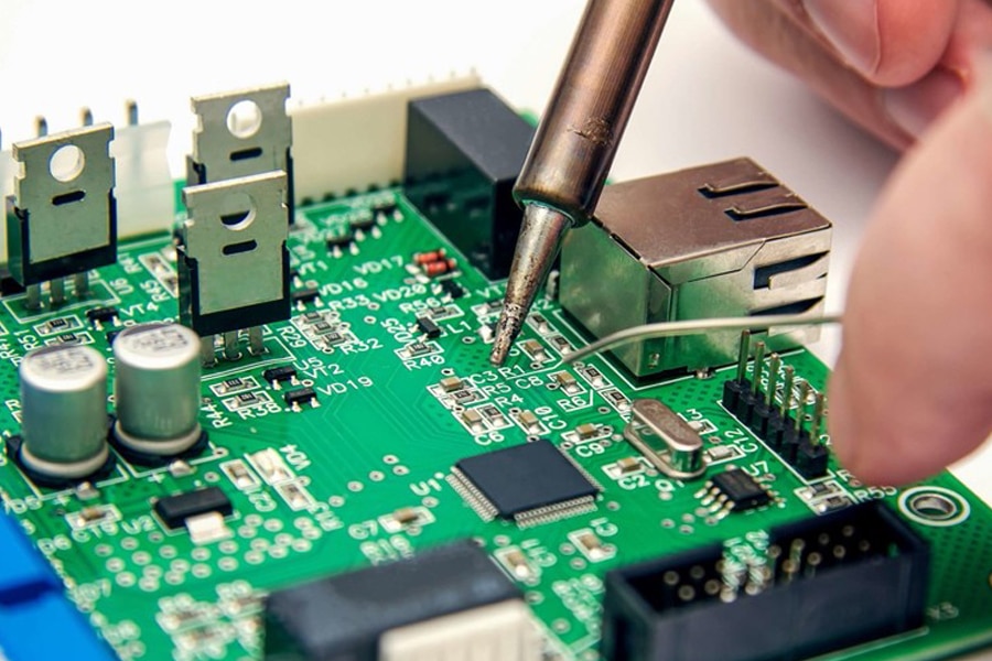
The application techniques for solder masks on a 2 layer HAL PCB can greatly influence the final product’s quality and reliability. The two primary methods for applying solder masks are screen printing and automated dispensing. Screen printing involves creating a stencil of the desired solder mask pattern and then using a squeegee to push the solder mask material through the stencil onto the PCB. This method is effective for high-volume production runs, ensuring consistent application across multiple boards.
Automated dispensing, on the other hand, is ideal for low-volume or prototype runs where precision is critical. This technique allows for better control over the amount of solder mask applied, reducing waste and ensuring coverage of only the necessary areas. Regardless of the method chosen, the solder mask must be applied uniformly to both sides of the 2 layer HAL PCB to prevent issues such as uneven curing or inadequate coverage, which can lead to defects during assembly or in the final product.
Challenges in Solder Mask Application for 2 Layer HAL PCB
While the application of a solder mask in a 2 layer HAL PCB is a crucial step in the manufacturing process, it is not without its challenges. One significant challenge is ensuring proper adhesion of the solder mask to the HAL finish. The HAL process involves coating the PCB with a layer of solder, which can sometimes create a surface that is less than ideal for solder mask adhesion. Manufacturers must employ specialized cleaning and surface treatment techniques to ensure that the solder mask adheres properly and forms a strong bond with the underlying materials.
Another challenge lies in the curing process. Proper curing of the solder mask is essential to achieve the desired physical and electrical properties. Incorrectly curing the solder mask can cause issues like delamination, discoloration, or reduced protection against environmental factors. Manufacturers must closely monitor the curing process, adjusting temperatures and times as needed to ensure that the solder mask on the 2 layer HAL PCB reaches its optimal state. These challenges necessitate a deep understanding of materials and processes, as well as a commitment to quality control throughout the manufacturing process.
Best Practices for Solder Mask Application
To ensure the highest quality solder mask application on 2 layer HAL PCBs, manufacturers should follow several best practices. First, thorough surface cleaning prior to solder mask application is critical to remove any contaminants that may interfere with adhesion. Next, manufacturers should thoroughly review solder mask specifications to determine the type best suited for a particular application. This includes considering factors such as heat and chemical resistance, as well as the PCB’s intended operating environment. Additionally, implementing rigorous quality control processes during the application and curing phases can help identify and mitigate potential issues early, ensuring that the final product meets or exceeds industry standards.
The Future of Solder Mask Application in 2 layer HAL PCB
The application of solder masks in 2 layer HAL PCBs is more than just a manufacturing step; it is a fundamental aspect that directly affects the reliability and efficiency of electronic devices. As technology advances and the demand for more complex and miniaturized electronic products increases, the role of solder mask application will become more critical. Understanding the intricacies of this process will enable designers and consumers to make informed choices that meet their performance and quality requirements.