What is the hdi layout of HDI PCB?
HDI PCB represents the progress of circuit board technology. These circuit boards aim to adapt to complex designs in a compact space, making them very suitable for modern electronics. When discussing HDI PCB, one of the most critical aspects is the HDI layout. This refers to how PCB’s layers, components, vias and traces maximize performance and efficiency. Knowing the HDI PCB’s HDI layout is essential for anyone who wants to work or cooperate with these high-performance boards. In this article, we will explore the key features and precautions involved in the HDI PCB’s HDI layout and explain how they affect the final product’s design, function and performance.
The Core Principles of HDI PCB Layout Design
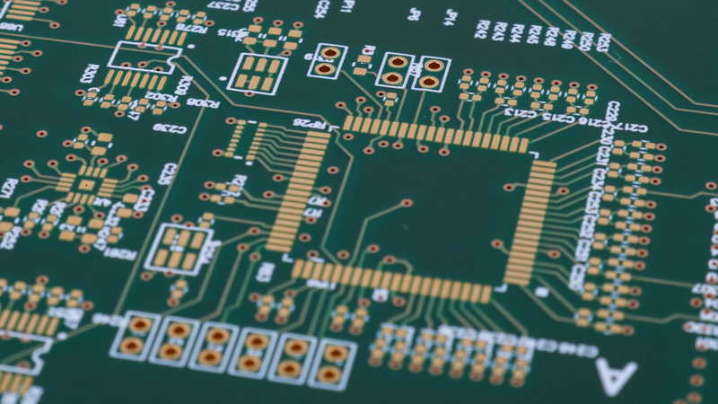
The layout of an HDI PCB is critical to its functionality, and designing it requires precise planning and consideration of various factors. One of the core principles of HDI PCB layout is layer density. HDI PCBs feature multiple layers, often with fine traces and small holes. These boards use advanced techniques such as micro vias, blind, and buried vias to connect these layers. The arrangement of these vias plays a crucial role in the overall layout. Microvias, in particular, are essential to HDI PCBs because they allow for more efficient use of space and help maintain the signal integrity of high-speed designs.
Moreover, the trace width and spacing in an HDI PCB layout must be precise. There is less room for error with smaller form factors and higher layer densities. Trace widths are calculated based on current carrying capacity, signal integrity, and impedance control. Additionally, the layout must consider component placement to minimize signal loss and interference while maintaining proper thermal dissipation.
Impact of Layer Stackup on Layout
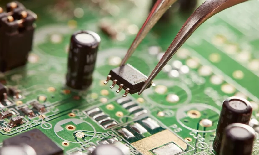
An essential aspect of the HDI PCB layout is layer stacking. In a traditional PCB, space and the available technology for connecting layers typically limit the number of layers. However, HDI technology makes it possible to have more layers in a smaller footprint. This is particularly important for devices that require dense circuit routing, such as smartphones or advanced medical devices. The more layers you stack within the board, the more complex the circuits become, allowing for improved functionality without increasing the board’s size.
When designing the HDI PCB layout, engineers decide how many layers are required and how these layers will interact. For example, a 4-layer HDI PCB may use a combination of micro vias to connect different layers, while a 6-layer HDI PCB might employ more advanced techniques like blind vias and buried vias to connect internal layers without using vias that go through the entire board. The stacking process also requires careful signal routing planning to prevent signal interference between adjacent layers.
The Role of Microvias and Vias in Layout
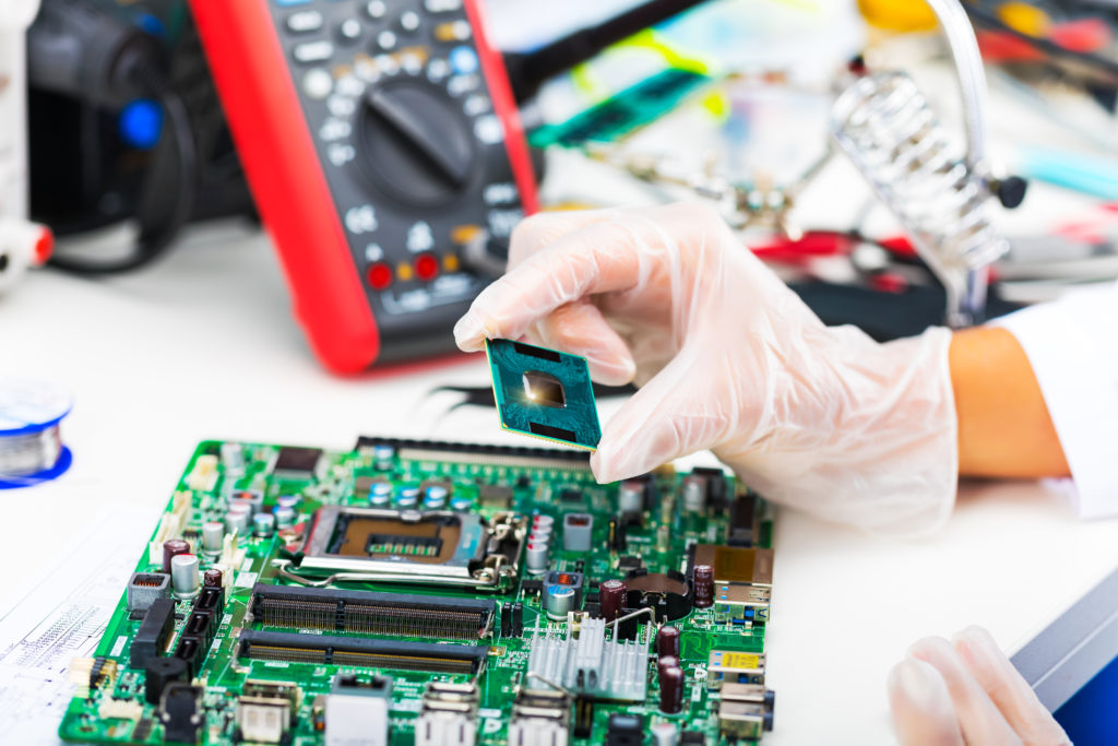
Microvias and vias are fundamental to the HDI PCB layout and contribute significantly to the board’s performance and miniaturization. Microvias are tiny, laser-drilled holes that connect layers in a compact space. These vias are much smaller than traditional vias, making them ideal for high-density designs. Designers often use microvias in HDI PCB layouts to connect the outer and inner layers, providing the flexibility to create more complex designs without increasing the overall board size. This is especially important for applications with limited space, such as wearable electronics and mobile devices.
In addition to micro vias, designers often use blind and buried vias in HDI PCB layouts to connect internal layers without compromising space on the outer layers. Blind vias extend from the outer layers to one or more inner layers, while buried vias connect only the internal layers, leaving the outer layers free for component placement. These technologies allow for more efficient use of space and better signal routing, which is crucial for maintaining the integrity of high-speed signals.
Component Placement and Its Impact on Layout
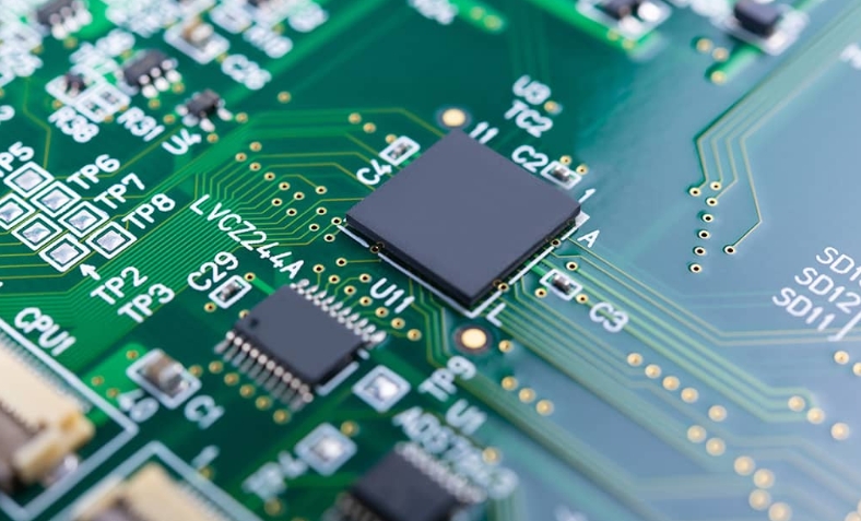
Another critical element of the HDI PCB layout is component placement. The arrangement of components on a PCB is crucial for minimizing signal interference, optimizing performance, and ensuring the board’s manufacturability. In HDI PCBs, where space is at a premium, efficient component placement becomes even more critical.
The placement of components in an HDI PCB layout must consider factors such as signal integrity, thermal management, and electromagnetic interference (EMI). Components that generate heat, for example, should be placed in areas with good thermal dissipation properties, while sensitive components should be shielded from high-frequency signals that could cause interference. Additionally, high-speed components such as processors or memory chips must be placed in a way that minimizes signal loss and crosstalk. In HDI PCB design, components are often placed in a compact, stacked manner to maximize space.
Thermal management is an essential consideration in layout.
Thermal management is crucial in the HDI PCB layout, especially for high-performance applications. To manage heat effectively, the HDI PCB layout must incorporate thermal vias, heat sinks, and pads to direct heat away from sensitive components. Thermal vias are small vias specifically designed to conduct heat from the element to other board layers, where it can be dissipated. In some cases, engineers use additional heat dissipation methods, such as external heat sinks or thermal pads, to improve thermal performance further.
When designing the layout, engineers must carefully consider the placement of power components and ensure that thermal vias surround them to channel heat away. Additionally, designers must ensure that the overall layout allows for efficient airflow and heat dissipation, particularly for high-power devices like processors and power management chips.
The Benefits of HDI PCB Layouts in Modern Electronics
The HDI PCB layout offers significant benefits, particularly for critical space, performance, and miniaturization industries. By incorporating advanced via technologies, compact layer stacking, and optimized component placement, HDI PCBs can achieve high performance in a smaller footprint compared to traditional PCBs.
HDI layouts are particularly beneficial in the consumer electronics, automotive, medical, and telecommunications sectors. Devices such as smartphones, tablets, wearables, and automotive control systems rely on HDI PCBs to meet the demands for high-speed processing, compact design, and durability. These boards offer improved signal integrity, reduced interference, and better thermal management, which is essential for maintaining the performance and reliability of modern devices. Additionally, the trend toward smaller, lighter devices in industries like wearable technology and IoT (Internet of Things) makes HDI PCBs a perfect solution.
The Essential Role of HDI PCB Layouts in Modern Electronics
The HDI PCB layout is integral to modern electronics, providing a compact yet high-performance solution for various applications. From optimizing layer stacking and via placement to managing heat dissipation and ensuring signal integrity, the HDI layout enables designers to create advanced, reliable, and efficient circuits. The demand for smaller, faster, and more powerful devices will only increase as technology evolves. The HDI PCB layout will be critical in meeting these demands, ensuring that electronics can advance without compromising performance.

