Are there limitations on component density with 2 layer HAL PCB?
As a leading manufacturer specializing in 2 layer HAL PCBs, we often receive questions about component density limitations. Component density is a critical factor in PCB design, determining how many components can be placed within a given area and how effectively these elements can perform together. Here, we explore the limitations of component density on 2 layer HAL PCBs, how this impacts design flexibility, and strategies that make this PCB type suitable for many applications.
Basics of Component Density in 2 Layer HAL PCB
Component density is one of the most essential considerations in PCB design, especially for 2 layer HAL PCBs. It refers to the number of components that can be integrated into a PCB while maintaining proper functionality and durability. Several factors affect component density in a 2 layer HAL PCB, including the available copper layers, trace layout, and heat dissipation properties. Since these PCBs have only two copper layers, designers face inherent limitations in how many components they can fit within a given space without compromising quality and performance.
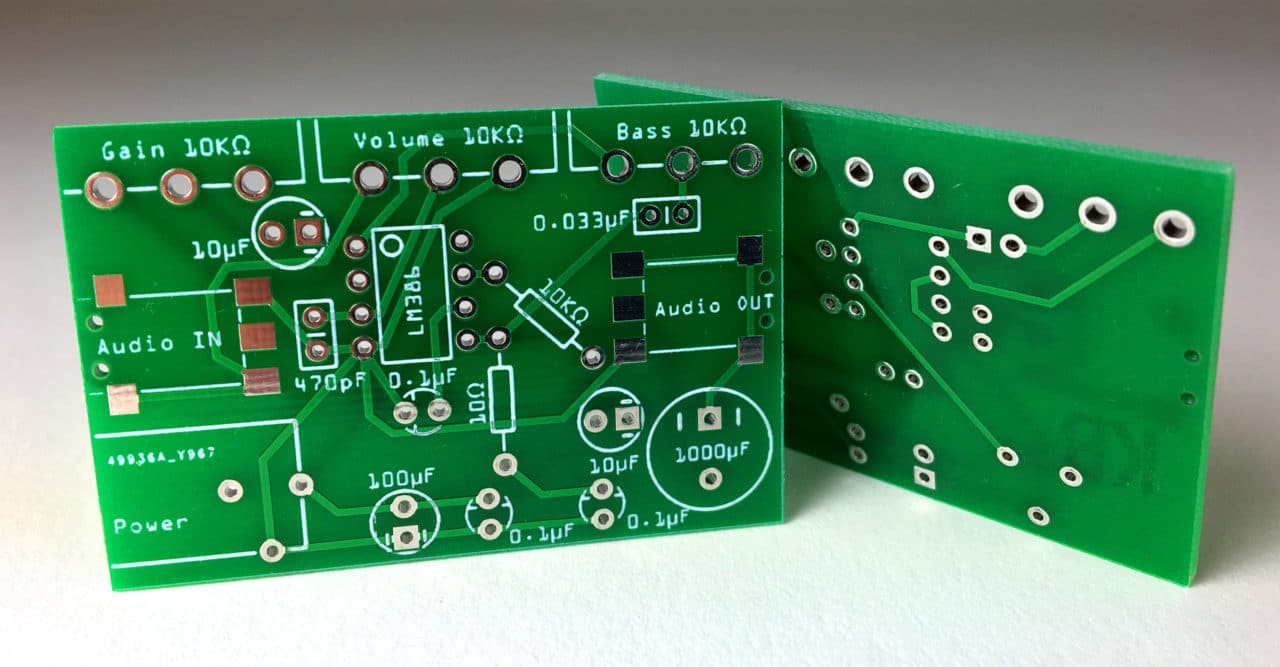
With only two conductive layers, routing paths are more limited than in multilayer boards. However, this simplicity also makes 2 layer HAL PCBs an ideal choice for many straightforward applications. Engineers can use clever layout techniques to create efficient designs for low-to-moderate density applications, keeping costs down while achieving reliable performance.

Routing Challenges When Designing PCBs
Routing in 2 layer HAL PCBs requires careful planning due to the limited number of conductive layers. In multilayer boards, designers can use additional layers to route signals and distribute power effectively. However, in a 2 layer HAL PCB, all routing must be completed on two surfaces, necessitating skillful layout techniques to avoid trace overlap, crosstalk, and signal interference.
Despite these challenges, 2 layer HAL PCBs remain highly popular in the electronics industry. Focusing on efficient routing techniques allows these boards to achieve effective component density while maintaining performance. Techniques such as minimizing via use, optimizing trace width, and employing surface-mount technology (SMT) components help designers maximize the available space on a 2 layer HAL PCB without creating noise or heat issues that would interfere with operation.
Cost Efficiency vs Component Density
One of the primary benefits of using 2 layer HAL PCBs is cost-effectiveness. Unlike multilayer boards, which are more expensive to produce, 2 layer HAL PCBs offer a more straightforward structure that leads to lower production costs. While this design may restrict component density, the balance of low cost and moderate density is ideal for many applications. Manufacturers widely use 2-layer HAL PCBs in products that do not require highly dense component placement or complex circuitry.
Cost efficiency is essential for manufacturers who aim to produce consumer electronics, automotive components, or prototypes with limited budgets. Although 2 layer HAL PCBs may not support as high a component density as multilayer boards, they provide an economical solution for projects where high density isn’t necessary. The ability to produce functional, reliable electronics without a high-density layout makes 2 layer HAL PCBs an intelligent choice for specific consumer applications.

Common Applications of PCBs with Medium Component Density
Given their structural simplicity, 2 layer HAL PCBs are best suited for applications that do not require extensive component density or multi-functional designs. Manufacturers commonly use these PCBs in devices like remote controls, power supplies, and specific consumer electronics, where basic functionality suffices. Moderate component density is typically sufficient for these applications, enabling smooth and stable performance without intricate routing.
In applications where space and weight constraints aren’t a priority, 2 layer HAL PCBs provide ample component density. They are instrumental in industries such as automotive, home automation, and even wearables, where simple circuits can function efficiently with lower density. With careful design, 2 layer HAL PCBs can also serve specific industrial uses, proving that moderate density isn’t necessarily a drawback but a strategic decision based on application requirements.
Maximizing Component Density on a 2 Layer HAL PCB
For users needing to achieve higher component density on a 2 layer HAL PCB, several techniques can help maximize the layout. Compact component placement, reduced usage, and employing SMT components are vital strategies. SMT components mount directly onto the board’s surface, allowing for greater density than traditional through-hole components, saving space and improving reliability.
Another method is to use smaller, more advanced components that support multiple functions within a single package. By doing so, designers can increase functionality without consuming additional board space. Additionally, custom layout techniques, such as the use of diagonal traces, can enhance component density in 2 layer HAL PCBs. Although a 2-layer board has limits on population density, these methods offer flexibility for higher-density requirements within the constraints of a two-layer system.

Comparing 2 Layer HAL PCB with Multi-Layer PCB Options
When comparing 2 layer HAL PCBs to multilayer boards, it’s essential to understand the trade-offs between density, cost, and complexity. Multilayer boards allow for higher density due to the additional routing paths available in their extra layers. These extra layers support advanced functionalities and increased thermal management capabilities, making multilayer boards ideal for devices that require complex or high-density layouts.
In contrast, 2 layer HAL PCBs excel in applications with acceptable simpler designs. The lower cost, ease of manufacture, and reduced weight make them preferable for basic consumer electronics, toys, and specific industrial controls. The choice between a 2 layer HAL PCB and a multilayer PCB ultimately depends on the user’s particular needs. A multilayer board may be necessary if high-density routing and advanced functionalities are required. However, a 2 layer HAL PCB often meets the requirements for cost-effective, low-to-moderate density projects.
Choosing the Right PCB for Your Component Density Needs
2 layer HAL PCBs provide a balanced solution for projects that require moderate component density at an affordable price point. While they present limitations regarding routing complexity and density compared to multilayer boards, they still offer substantial versatility across various applications. By understanding the density requirements of your project and the benefits of using 2 layer HAL PCBs, you can make an informed decision that supports both your design goals and budget.

