Can 8-layer SSD PCB integrate power and signal layers?
As the demand for faster, more efficient, and more compact storage solutions continues to grow, manufacturers are constantly innovating in the design of printed circuit boards. An 8-layer SSD PCB is a prime example of how technological advancements have enabled the integration of power and signal layers to improve performance and reliability. This blog post explores whether 8-layer SSD PCBs can integrate power and signal layers, delving into the design challenges, benefits, and real-world applications.
Overview of 8-layer SSD PCB
An 8-layer SSD PCB is a high-density, multi-layer circuit board for solid-state drives (SSDs). It features eight distinct layers that alternate between signal, power, and ground planes to manage data transmission, power delivery, and thermal performance.
Each layer in an 8-layer SSD PCB serves a specific purpose, contributing to its complex design. Signal layers manage data pathways, while power and ground layers distribute energy and minimize noise. This intricate configuration ensures a compact design that meets the high-speed requirements of SSDs, which are increasingly used in laptops, servers, and gaming systems. The design of an 8-layer SSD PCB is not just complex, but it also offers unmatched benefits. With a well-balanced stack-up, these PCBs can maintain signal integrity, reduce electromagnetic interference (EMI), and deliver stable power—essential features for devices operating at gigabit speeds.
The Advantages of Integrating Power and Signal Layers
The benefits of integrating power and signal layers in an 8-layer SSD PCB are substantial. The most significant advantage is the improved space efficiency. By sharing layers between power distribution and signal routing, designers can achieve a compact form factor without compromising functionality.
Another benefit is enhanced signal integrity. Power and ground planes act as shields, reducing crosstalk and interference between adjacent signal traces. This is particularly important for high-speed applications, where even minor disruptions can affect performance.
Thermal management also improves with integration. Power layers can double as heat dissipation surfaces, spreading thermal energy across the PCB to prevent overheating. This ensures reliable operation, especially in environments with limited airflow. Lastly, integrated designs simplify manufacturing. Fewer layers dedicated exclusively to power or signal functions mean reduced costs and production complexity, making them an attractive option for manufacturers.
Key Design Challenges for 8-Layer SSD PCBs
While integration offers advantages, it also introduces design challenges for 8-layer SSD PCBs. One major challenge is balancing signal and power distribution. Combining these functionalities requires precise layer stack-up planning to avoid conflicts.
For example, poorly placed power traces can create noise that interferes with high-frequency signals. Designers must carefully route these traces and use decoupling capacitors to stabilize voltage levels.
Heat management is another challenge. With power layers generating heat, improper thermal design can lead to performance issues. Advanced simulations and thermal via placement help mitigate these risks. Moreover, integrating power and signal layers increases the complexity of impedance control. High-speed data signals require strict impedance matching to maintain performance, which is harder to achieve when layers serve multiple functions.
The Role of Stack-Up in Power and Signal Integration
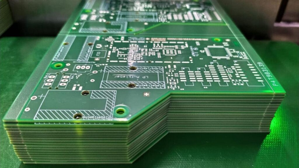
The stack-up configuration is critical when designing an 8-layer SSD PCB that integrates power and signal layers. A typical configuration might alternate signal layers with power and ground planes, ensuring optimal isolation and noise suppression.
For instance, placing a ground plane adjacent to a signal layer reduces EMI by providing a stable reference point. Similarly, having power layers adjacent to ground planes helps maintain voltage stability. This layered approach minimizes interference and improves overall PCB performance. Advanced software tools like Cadence Allegro and Altium Designer allow engineers to model and optimize these stack-ups. By simulating electrical performance and thermal behavior, designers can identify potential issues before manufacturing, ensuring a reliable and efficient PCB.
Practical applications and cases
The practical benefits of 8-layer SSD PCBs are evident in cutting-edge products. For example, the Samsung 970 Evo Plus SSD leverages an advanced PCB design to deliver exceptional read/write speeds. Its integrated power and signal layers contribute to its compact size and performance efficiency.
Similarly, the Western Digital SN850 NVMe SSD uses an 8-layer PCB with integrated features to achieve superior thermal management and high-speed data transfer. These designs demonstrate how integrated PCBs enable manufacturers to meet consumer demands for faster, smaller, and more reliable storage solutions. Such applications underline the importance of collaboration between designers, engineers, and manufacturers to achieve seamless integration.

Innovations in 8-Layer SSD PCB Manufacturing
Modern manufacturing techniques have made producing 8-layer SSD PCBs with integrated power and signal layers easier. Techniques like laser drilling allow for the creation of microvias, which connect layers without consuming excess space.
Additionally, direct imaging technology ensures precision in trace patterns, which is essential for maintaining signal integrity at high speeds. Advances in copper plating and dielectric materials also enhance the performance and reliability of these PCBs.
Future innovations, such as AI-driven design tools and additive manufacturing, promise to simplify the production process further. These technologies will make integrated designs more accessible to manufacturers, driving wider adoption across industries.
Pioneering the Next Era of SSD PCB Integration
The future of 8-layer SSD PCB design lies in greater integration and innovation. As data transfer speeds increase with technologies like PCIe Gen5, the need for efficient PCBs will grow.
Emerging materials with lower dielectric constants will support these advancements, enabling better signal integrity at higher frequencies. Additionally, features like embedded sensors for thermal monitoring and adaptive power distribution are expected to become standard in next-generation SSD PCBs.These developments will empower manufacturers to create even more compact, efficient, and robust storage solutions, pushing the boundaries of what SSDs can achieve.
The Potential of 8-Layer SSD PCB
Integrating power and signal layers in an 8-layer SSD PCB is a game-changer for the storage industry. This design approach offers a compact, efficient, high-performance solution for modern applications. With continuous innovation in materials, design, and manufacturing, the potential of 8-layer SSD PCBs is limitless, paving the way for faster and more reliable storage solutions.

