
Can Gold Finger PCB support high-density interconnection?
The demand for high-density interconnect (HDI) PCBs is growing exponentially in today’s rapidly evolving electronics market. HDI PCBs are essential in telecommunications, consumer electronics, medical devices, and automotive systems. They can integrate multiple layers of circuitry in a compact space, enabling more functionality in a smaller form factor. A key component of many HDI PCBs is the gold finger PCB. This article will explore the relationship between gold finger PCBs and high-density interconnects, delving into the key aspects of the design and functionality of these PCBs in advanced electronic systems.
A Brief Introduction to High-Density Interconnects
High-density interconnection (HDI) refers to creating printed circuit boards with finer lines, smaller vias, and more layers, facilitating higher component densities. HDI PCBs are characterized by their ability to accommodate complex designs in smaller spaces, allowing for increased functionality while minimizing physical space requirements. This process often includes micro vias, blind vias, and buried vias, which are smaller in size and designed to carry signals through multiple layers of a PCB.
HDI technology is critical for modern devices that demand advanced functionality and performance. As consumer electronics, telecommunications equipment, and automotive systems evolve, the need for HDI boards to handle high-speed data transmission and complex features increases. Gold Finger PCBs support these advanced designs by providing reliable interconnections, especially for high-speed data transfer applications.
The Role of Gold Fingers in PCB Design
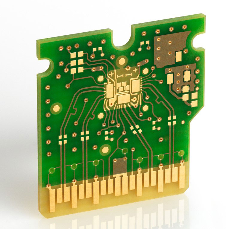
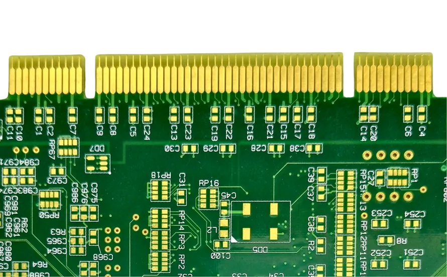
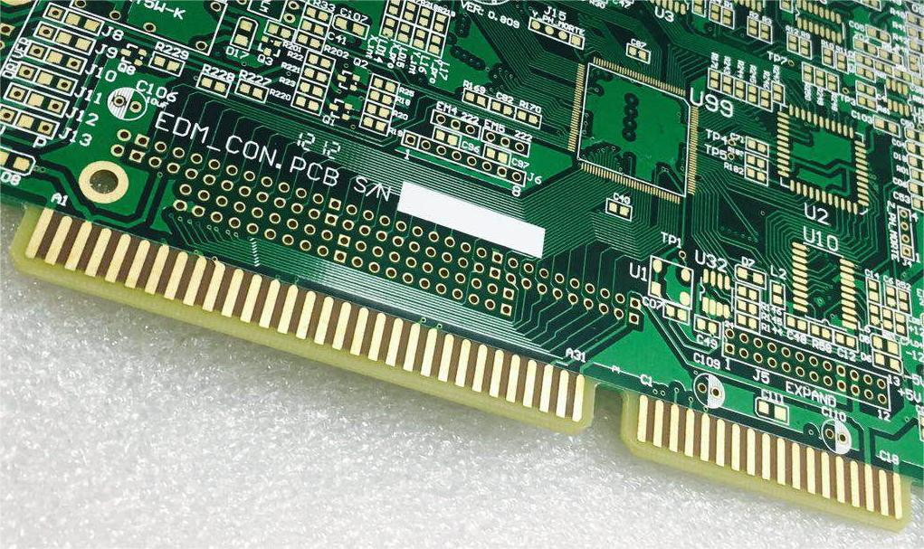
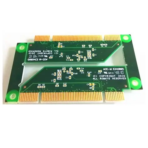
Gold fingers are the metal contacts at the edge of Gold Finger PCBs, commonly used to connect a PCB to external devices. These gold-plated contact points provide reliable connections to connectors, ensuring a stable electrical signal transfer. Gold fingers are especially beneficial for high-frequency applications, as they offer excellent corrosion and low contact resistance, making them ideal for high-density interconnections in modern PCBs.
These gold-plated edges are integral to devices that require high-speed data transfer, such as network equipment, gaming consoles, and servers. Manufacturers can use gold fingers to ensure a robust electrical connection, allowing the PCB to support high-density designs and complex electrical signals. As Gold Finger PCBs evolve, they enable increasingly sophisticated designs that are space-efficient and reliable in handling intricate interconnections.
Are Gold Finger PCBs suitable for Handling High-Density
Yes, Gold Finger PCBs are well-suited to handle high-density interconnections. Their key feature is their ability to accommodate the intricate circuitry and connection points required for HDI applications. By using micro vias, high-density interconnection can be achieved through the use of fine traces and smaller vias, all while ensuring reliable and consistent electrical connections at the edge of the PCB.
The gold fingers, which serve as the primary contact points for connectors, are designed to provide low-resistance, high-reliability connections. This is critical when designing HDI circuits that require precise, high-speed data transmission. The high-quality plating process for gold fingers ensures they can withstand the electrical stresses typically encountered in high-density designs, thus supporting faster, more reliable signal transfer in complex, multi-layer PCBs.

Key Factors for Supporting High-Density Interconnection
Several factors contribute to Gold Finger PCBs’ ability to support high-density interconnections. The first is the use of advanced manufacturing techniques such as microvia technology. Microvias are small, laser-drilled holes allowing multi-layer interconnections while minimizing the space used on the PCB. This is particularly important in HDI designs, where every square millimetre counts.
In addition to microvias, the use of fine trace widths and high-performance dielectric materials also plays a role in supporting high-density interconnection. Fine traces reduce the amount of space occupied by each signal line, allowing for the accommodation of more connections within the same physical area. The choice of materials also impacts the performance of the PCB, especially in high-speed applications. High-frequency PCB materials, such as PTFE or ceramic-based substrates, often ensure low signal loss and minimal crosstalk in HDI designs.
The Impact of Gold Finger Technology on Signal Integrity
Signal integrity is crucial in HDI applications. As electronic devices become more complex, the need for reliable signal transmission becomes even more important. Gold Finger PCBs contribute significantly to maintaining signal integrity in high-density interconnection designs by providing stable, low-resistance connections.
Gold is an excellent conductor, and its use as gold fingers ensures that signals are transmitted with minimal loss or interference. The durability of the gold plating also means that these connections can withstand the wear and tear of frequent use, maintaining high performance over time. This is especially important in high-speed circuits that rely on precise signal timing to ensure proper operation. This way, Gold Finger PCBs enable devices to function reliably even under demanding conditions.
The Advantages of Using Gold Finger PCBs for High-Density Applications
There are several advantages to using Gold Finger PCB in high-density interconnection applications. The most notable advantage is creating robust, high-speed connections in compact spaces. This is particularly useful in telecommunications, where devices must handle large amounts of data while maintaining a small form factor.
Gold fingers also help improve the PCB’s overall longevity and reliability. The gold plating provides excellent corrosion resistance, ensuring that the contacts will remain in good condition for extended periods. This is important in applications where frequent or continuous signal transmission is required, such as communication systems or high-performance computing devices.
Furthermore, gold fingers can facilitate easy connections to external components, such as connectors, which can simplify the assembly process and reduce the overall cost of manufacturing.
Applications That Benefit from High-Density Interconnection and Gold Finger Technology
Gold Finger PCBs are commonly used in various applications with critical high-density interconnections. These include network equipment, telecommunications hardware, servers, and consumer electronics like gaming consoles and smartphones. In these applications, fitting more connections into a smaller space without compromising performance is essential.
In addition to consumer electronics, industries such as aerospace, automotive, and medical devices also benefit from high-density interconnections. Gold Finger PCBs are used in these fields to connect sensors, communication modules, and other complex systems that require reliable, high-speed data transfer. Their robustness makes them ideal for environments where physical and electrical stress is prevalent.
Gold Finger PCB is Essential for High-Density Interconnections
Gold Finger PCBs are a key enabler of high-density interconnection in modern electronic devices. They can support micro vias, fine traces, and advanced materials, helping facilitate the compact, high-performance designs required in today’s fast-paced technological landscape. The gold plating used in the fingers ensures reliable, low-resistance connections that are crucial for high-speed, high-frequency applications. Whether in telecommunications, automotive, or consumer electronics, Gold Finger PCBs provide the essential connection points that enable high-density interconnection. As electronic devices continue to shrink while increasing in functionality, the role of Gold Finger PCBs in supporting these complex designs will remain critical to the success of modern technology.