What are the most common gold plating methods for gold finger PCB?
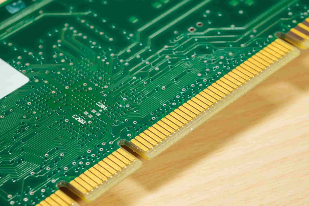
The Gold finger PCB is an indispensable component in the electronics industry. It can be used as a connector to provide a reliable interface between different electronic devices. These specialized PCBs have gold-plated contacts, called gold fingers, which ensure safe and efficient connections. The gold plating process improves these connectors’ performance and service life, making them indispensable to high-performance applications such as telecommunications, automotive electronics, and data transmission systems. Next, we will introduce you to several gold plating methods for gold finger PCBs.
Electroplating: A Widely Used Method for Gold Finger PCB
They commonly use electroplating for gold-plating finger PCBs. This process uses an electric current to deposit a thin layer of gold onto the copper connectors of the PCB. The PCB is submerged in a gold salt solution, and the electric current causes gold ions to bond with the copper surface. This highly efficient process scales easily for mass production, making it ideal for high-volume manufacturing.
The benefits of electroplating for gold finger PCBs include precise control over the thickness of the gold layer, ensuring optimal conductivity and performance. By adjusting the plating time and current, manufacturers can fine-tune the thickness of the gold to meet specific requirements. Electroplating is also versatile, offering excellent uniformity and high-quality results, making it suitable for large-scale production in consumer electronics and telecommunications industries.

Electroless Plating: Achieving Uniform Gold Coating Without Electricity
Electroless plating is another popular gold plating method used for gold finger PCBs. It does not require an electric current to deposit gold. Instead, a chemical reaction initiates the deposition of gold ions onto the PCB’s surface. This process allows for a uniform gold coating, even complex and intricate PCB designs.
The advantage of electroless plating for gold finger PCBs is its ability to create a consistent and uniform gold layer without the need for precise electrical control. This makes it particularly useful for PCBs with non-flat or irregular surfaces. Electroless plating ensures high-quality plating, even in areas that are difficult to reach, using other methods, such as holes or narrow spaces. It is ideal for precision applications that require consistent and reliable gold plating.
Immersion Gold: Provides Superior Durability
Immersion gold is a widely used gold plating method for gold finger PCBs that provides enhanced durability and resistance to corrosion. In this process, the PCB is immersed in a gold-plating solution, and a thin layer of gold is deposited onto the PCB’s connectors. Manufacturers often apply a nickel layer first to improve the adhesion of gold to the surface and prevent corrosion.
One of the primary advantages of immersion gold for gold finger PCBs is its ability to offer superior protection against oxidation and environmental factors. The gold layer provides a highly durable, long-lasting finish that ensures the connectors maintain their functionality over time. Immersion gold is particularly beneficial in industries where long-term reliability is essential, such as medical devices, automotive electronics, and telecommunications equipment.

Comparing several plating Methods
When choosing the correct gold plating method for gold finger PCBs, it’s important to consider the application’s specific requirements. Electroplating is often the preferred choice for high-volume manufacturing, as it is cost-effective and allows precise control over the gold thickness. It is ideal for consumer electronics, where uniformity and efficiency are key factors.
On the other hand, electroless plating is a better choice for PCBs with intricate designs or irregular surfaces. Its ability to deposit gold evenly across complex shapes ensures consistent performance. While typically more expensive than other methods, immersion gold offers superior durability and protection against oxidation, making it the best choice for long-term reliability applications.
Benefits of Gold Plating for Gold Finger PCBs
Gold plating ensures gold finger PCBs’ performance, longevity, and reliability. Gold offers excellent electrical conductivity, improving signal integrity and reducing interference risk. This is particularly important in high-speed applications, where maintaining the signal’s integrity is critical.
In addition to enhancing conductivity, gold plating provides superior protection against corrosion and oxidation. Gold’s resistance to environmental degradation ensures that gold finger PCBs continue functioning effectively over time, even in harsh or humid environments. This makes gold-plated connectors ideal for use in industries such as telecommunications, automotive, and medical devices, where long-term performance is essential.

Choosing the Right Gold Plating Method for Your Gold Finger PCB
Selecting the most appropriate gold plating method for gold finger PCBs depends on factors such as production volume, application requirements, and cost considerations. Manufacturers widely use electroplating for large-scale production because it is efficient and cost-effective. It is ideal for industries where high-volume manufacturing is essential, such as consumer electronics.
Electroless plating is a more specialized method when uniformity and precision are required, particularly for complex designs. It is ideal for high-performance applications where the gold layer must be consistent and uniform across the PCB. Immersion gold is the best choice for applications that require long-term durability and corrosion resistance, such as medical or aerospace devices. Understanding the strengths and weaknesses of each method will help you choose the best solution for your gold finger PCB needs.
Proper gold plating is critical for gold finger PCBs
The choice of gold plating method is crucial to the performance and reliability of gold finger PCBs. Each plating method—electroplating, electroless plating, or immersion gold—offers distinct advantages depending on the application’s specific needs. Understanding these methods and their benefits will allow you to select the most appropriate solution for your gold finger PCB.
