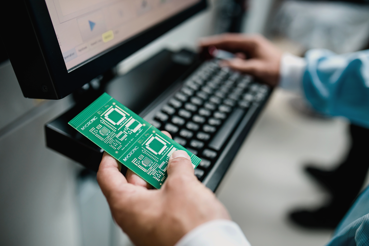
What is the process for designing and manufacturing double-sided PCB?
PCBs are essential components in almost all electronic devices today. Double-sided PCBs, in particular, stand out for their versatility, compact design, and cost-effectiveness. These PCBs allow engineers to mount components on both sides of the board, maximizing available space and enabling more complex circuit designs. In this blog post, we will guide you through designing and manufacturing a double-sided PCB.
The Basics of Double-Sided PCB Design
Designing a double-sided PCB starts with planning, where engineers define the circuit layout, component placement, and connection requirements. Double-sided PCBs are designed to mount electrical components on both the top and bottom sides of the board, requiring careful planning to ensure clear paths for electrical connections on both sides.
The first step in the design process involves creating a schematic diagram that represents the circuit and shows how each component connects. This diagram acts as a blueprint for the PCB layout. Engineers use design software such as Eagle or Altium Designer to convert the schematic into a layout, which includes routing traces and placing components.
One key challenge in designing double-sided PCBs is optimizing the use of both sides of the board. Designers must place components efficiently to avoid interference or short circuits. Additionally, the design must consider the need for vias, which are small holes that allow traces to pass from one side of the board to the other.
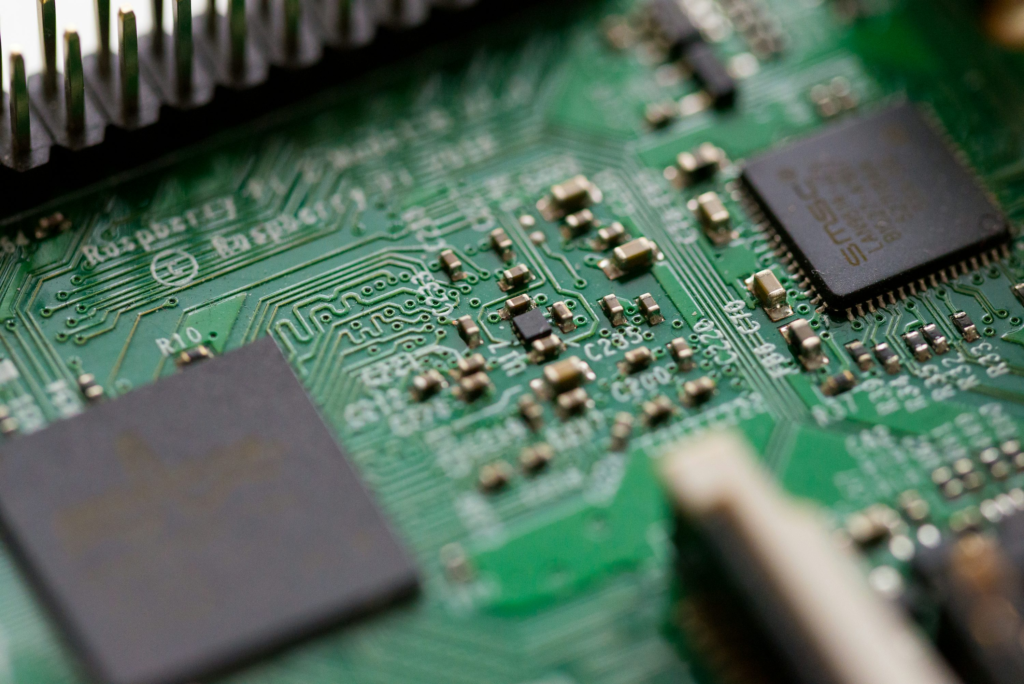
PCB Layer Stack-Up and Material Selection
After completing the initial design, the next step involves determining the layer stack-up and selecting the right materials for the double-sided PCB. The layer stack-up refers to the number of copper and dielectric material layers used in the board. For double-sided PCBs, the board typically consists of two copper layers, one on the top and one on the bottom.
The choice of materials is critical because it directly affects the PCB’s performance and durability. The most common material for the PCB substrate is FR4, a fibreglass-reinforced epoxy laminate. FR4 is cost-effective, durable, and offers good insulating properties, making it ideal for many types of PCBs.
Designers may opt for specialized materials like Rogers or Teflon for high-frequency or high-performance applications. These materials offer better signal integrity and lower loss but come at a higher cost. Material selection must align with the device’s requirements, balancing cost, performance, and durability.
The Process of Creating the PCB Layout
With the design finalized and materials selected, the next step in manufacturing a double-sided PCB is creating the PCB layout. This is where the physical aspects of the PCB begin to take shape. The design specifies the placement of components, traces, pads, vias, and other necessary elements on both sides of the board.
At this stage, engineers transfer the design to a computer-aided design (CAD) file, which is used for fabrication. They carefully examine the layout to ensure that all electrical connections are correct and that no spacing or trace width issues exist. They also verify that vias are positioned correctly for efficient connections between the two sides of the board.
One challenge in creating a double-sided PCB layout is ensuring optimal use of both sides. Designers often use advanced techniques like blind and buried vias, which connect layers without passing through the entire board. Layout accuracy is critical for the final quality and performance of the PCB.
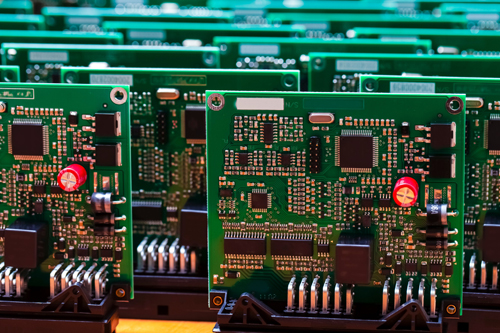
PCB Fabrication and Etching
Once the layout is complete and checked, the next step is fabricating the PCB. The process begins with preparing the substrate, usually a copper-clad laminate. Engineers coat the copper layers with a thin photoresist layer sensitive to ultraviolet (UV) light.
Engineers transfer the PCB design onto the photoresist-coated copper through a photolithographic process. This involves exposing the board to UV light through a mask containing the circuit design. The UV light exposes the photoresist, removing the exposed areas and leaving behind the desired pattern of copper traces.
After transferring the design, the next step is etching. A chemical solution removes the unexposed copper, leaving only the copper traces that form the circuit. This process is crucial for creating the intricate patterns needed for electrical connections on both sides of the board.
Drilling and Via Formation for Double-Sided PCB
A defining feature of double-sided PCBs is using vias to connect traces on the top and bottom sides of the board. Vias are small holes drilled through the board, allowing electrical connections to pass between the two layers.
Engineers use high-speed drilling machines to create these tiny holes. The size and placement of vias are critical to the performance and integrity of the PCB. Blind vias, which connect the outer layer to one or more inner layers without passing through the entire board, and buried vias, located within the layers and not visible from the surface, are often used in double-sided PCB designs.
After drilling, engineers plate the vias with copper to ensure electrical conductivity. The plating process involves an electrolytic solution that coats the inner walls of the vias with copper, allowing electrical signals to travel seamlessly between the top and bottom layers of the PCB.
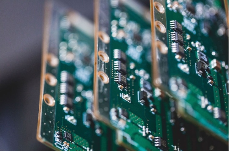
Solder Mask and Component Placement
Once the vias are formed, engineers apply the solder mask. The solder mask is a protective layer applied to the PCB’s surfPCB’so prevent short circuits and protect the copper traces. It also helps control solder flow during component assembly.
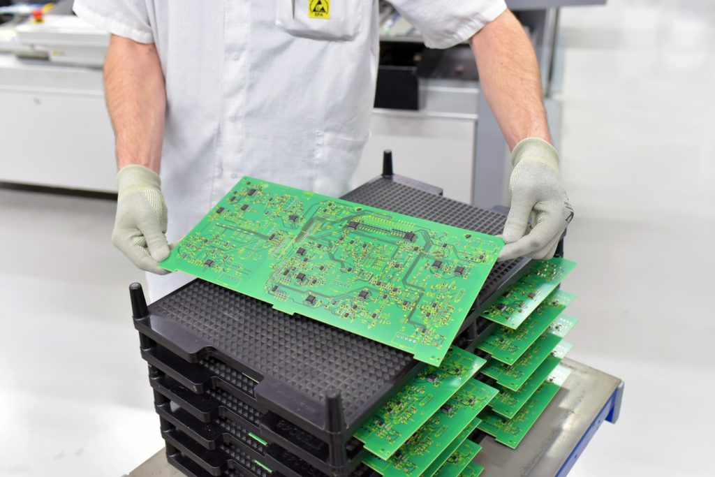
Typically green, the solder mask can also be red, blue, or black. Engineers apply the solder mask through a screen printing process, where the material is applied to the board, leaving only the pads and vias exposed. This step ensures that only designated board areas will be used for component placement and soldering.
After applying the solder mask, engineers proceed to component placement. This involves placing electronic components such as resistors, capacitors, and integrated circuits (ICs) onto the PCB. Automated pick-and-place machines typically handle this task, ensuring accurate component positioning on the board.
Testing, Quality Control, and Final Assembly
The final stage in manufacturing double-sided PCBs involves testing and quality control. After placing the components, the PCB undergoes several checks to ensure it meets design specifications. These include visual inspection, electrical testing, and functionality testing to verify that the PCB performs as expected.
Each PCB also undergoes a series of quality control procedures, including inspections for defects like misaligned components or poor solder joints. For the final assembly, engineers solder the components onto the PCB using wave soldering or reflow soldering, depending on the type of components used.
Once the PCBs are assembled and tested, they are packaged and prepared for shipment. The finished product is ready for use in various applications, from consumer electronics to industrial systems.
The Importance of Precision in Double-Sided PCB Manufacturing
Designing and manufacturing double-sided PCBs requires precision at every step. From the initial design to the final assembly, attention to detail and accuracy are crucial for producing high-quality PCBs that meet the demands of modern electronics. By understanding the process, users and consumers can better appreciate the value of investing in well-designed and manufactured double-sided PCBs. Whether creating consumer electronics, medical devices, or industrial equipment, high-quality PCBs form the foundation for reliable and efficient performance. The intricate manufacturing process ensures the final product is robust, efficient, and ready for use in various applications.

