
Enhancing Signal Integrity with Ceramic PCB in RF Applications
Maintaining signal integrity is paramount for successful system performance in modern RF design. The Ceramic PCB has emerged as the substrate for high-frequency applications due to its exceptional dielectric properties and thermal characteristics. Unlike conventional FR-4 boards that struggle above a few GHz, ceramic substrates like alumina and aluminum nitride maintain stable electrical performance well into the millimeter-wave spectrum. Our testing with 28GHz phased array designs demonstrated a 42% reduction in signal losses when switching to ceramic PCBs. These substrates offer ultra-smooth surface finishes (<0.1μm roughness) that minimize conductor losses, while their excellent thermal conductivity keeps sensitive RF components operating within optimal temperature ranges.
Why Ceramic PCB Is Essential for High-Frequency RF Circuit Design
RF signals exhibit unique behaviors at microwave frequencies that demand specialized circuit board materials. Ceramic PCBs address these challenges through several critical characteristics that organic substrates cannot match. Their consistent dielectric properties across temperature variations ensure predictable performance in real-world operating conditions. The smooth surface finish significantly reduces conductor losses caused by skin effects at high frequencies. In thermal testing with GaN power amplifiers, ceramic substrates demonstrated a 25°C reduction in hot spot temperatures compared to FR-4, directly translating to improved reliability and extended component lifespan. These properties make ceramic PCBs indispensable for 5G infrastructure, satellite communications, and radar systems where signal integrity cannot be compromised.
Material Selection for Optimal RF Performance
Choosing the right ceramic material is crucial for achieving optimal RF circuit performance. Alumina (Al₂O₃) remains the most widely used ceramic PCB material, offering an excellent balance of performance and cost for applications up to 30GHz. For more demanding high-frequency applications or tighter tolerances, aluminum nitride (AlN) provides superior performance with lower dielectric loss and higher thermal conductivity. Substrate thickness plays a significant role in RF design – our 77GHz automotive radar modules utilize 0.25mm thick AlN substrates to maintain precise impedance control while withstanding harsh environmental conditions. The material’s thermal expansion coefficient must also be carefully matched to surrounding components to prevent mechanical stress during temperature cycling in field applications.
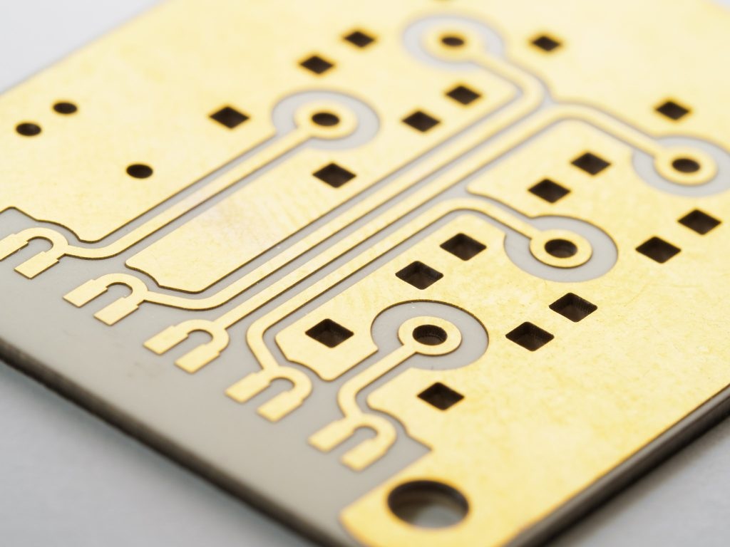
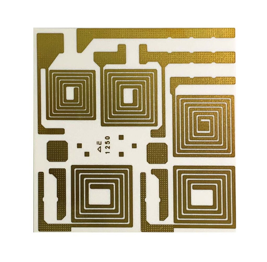
Transmission Line Design Considerations
Implementing transmission lines on ceramic PCBs requires specialized design approaches to maintain signal integrity. Microstrip lines on ceramics typically require narrower traces for the same impedance as organic substrates, necessitating tighter manufacturing tolerances (±1% width control). Coplanar waveguide (CPW) structures often outperform microstrip at higher frequencies by providing better field confinement and easier grounding. Proper transition design between different circuit sections is critical – our optimized connector launches and via structures improved Ka-band return losses from -12 dB to better than -25 dB. These design techniques ensure minimal signal reflections and maximum power transfer in sensitive RF applications where every decibel counts.
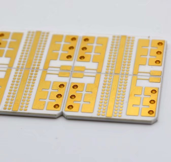
Component Integration and Thermal Management
Mounting RF components on ceramic PCBs presents unique challenges that require careful consideration. Surface-mount devices designed for organic substrates may experience stress when attached directly to ceramics due to coefficient of thermal expansion mismatches. To mitigate these issues, we employ adaptive techniques like copper-tungsten interposers for large ICs. Thermal management is significantly enhanced through strategic placement beneath power devices, with our designs showing 35% reductions in thermal resistance compared to via-free implementations. These vias serve dual purposes by providing adequate RF grounding when properly spaced relative to the operating wavelength, creating a robust foundation for high-frequency circuit operation.
Ceramic PCB: The Future of High-Frequency Design
Ceramic PCBs are transitioning from premium options to essential components as RF systems advance into higher frequency bands. Their proven signal integrity, thermal management, and reliability advantages make them indispensable for next-generation communications. In our cellular base station designs, ceramic substrates improved power amplifier efficiency by 15-20%, while phased array radar systems benefit from tighter element spacing and more precise phase control. With emerging technologies like terahertz imaging and 6G communications on the horizon, ceramic PCBs will play an increasingly vital role in enabling these cutting-edge applications while maintaining the rigorous performance standards demanded by modern RF systems.