Are there any specific design considerations when developing a smart ring flex PCB?
Wearable technology continues to develop rapidly, and bright rings have become a major player in the personal device space. Small, versatile, and feature-rich bright rings offer users a combination of fashion and utility. At the heart of these devices is the smart ring flex PCB, which enables these rings to operate efficiently in a tiny form factor. Several essential design factors must be considered when developing a smart ring flex PCB to ensure optimal performance, comfort, and reliability. These considerations cover everything from material selection to power consumption and integration with other components. In this blog post, we will explore the most critical design factors when developing a smart ring flex PCB and how these decisions affect the overall performance of the bright ring.
Core Considerations for Smart Ring Flex PCB
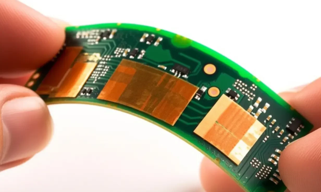
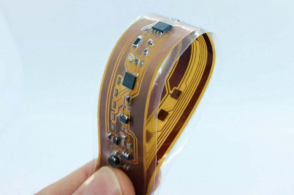
The main advantage of a flexible, bright ring PCB over a traditional rigid PCB is its flexibility, which makes the ring comfortable to wear and conforms to the natural curvature of the finger. Designing a flexible PCB that is both flexible and durable requires choosing the right materials. Typically, manufacturers use polyimide (PI) or polyester (PET) films as substrates because they offer excellent flexibility while being strong enough to withstand daily wear.
PCBs must withstand constant bending, twisting, moisture, heat, and sweat exposure for smart rings. Therefore, the materials must have high tensile strength, resist deformation, and maintain their functionality over time. In addition, the PCB’s flexibility mustn’t sacrifice durability. If the PCB is too fragile, it may result in signal transmission failure or mechanical failure over time. The right balance between flexibility and durability is a key design consideration when developing a flexible PCB for smart rings.

Miniaturization and Integration of Components in Smart Ring Flex PCB
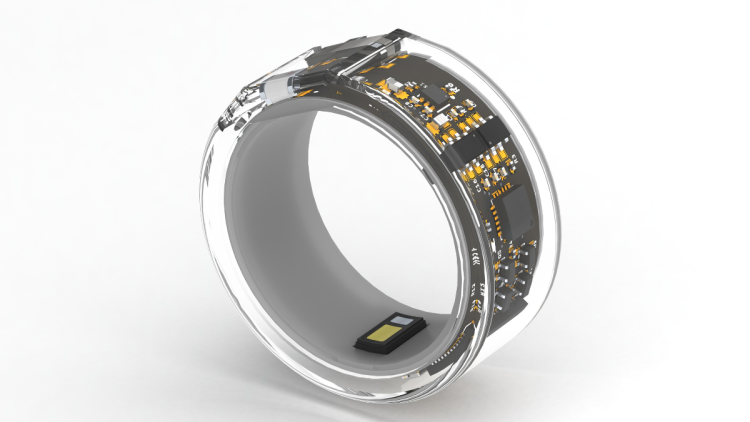
One of the most challenging aspects of designing a flexible smart ring PCB is the need for miniaturization. Given the smart ring’s small size, designers must carefully fit all components into the limited space without compromising performance. Integrating various electronic components, such as sensors, microcontrollers, antennas, and power management systems, into a compact layout.
To achieve this, designers typically employ multi-layer PCB designs, stacking components where necessary and using advanced packaging techniques such as chip-on-board (COB) to reduce the overall footprint of the circuit. These techniques help integrate small but essential components such as heart rate sensors, accelerometers, and gyroscopes into the PCB without making the bright ring too bulky. In addition, it is necessary to ensure that the bright ring flexible PCB maintains effective heat dissipation and signal integrity. With densely packed components, managing heat is critical to prevent damage to sensitive electronic devices. This can be achieved through careful layout design, thermal vias, or the installation of heat sinks in critical areas of the PCB.
Power Consumption and Energy Efficiency in Smart Ring Flex PCB Design
Smart rings typically rely on small batteries, which must be compact and lightweight to match the size of the ring. Given the space constraints, ensuring efficient power consumption and energy management is one of the most critical design factors for smart ring flex PCB development. A well-designed PCB must help minimize energy consumption while ensuring the device can operate continuously throughout the day.
The primary challenge is optimizing the power consumption of the various components, particularly sensors and wireless communication modules, often the most power-hungry elements of a bright ring. Designers must focus on power-saving techniques, such as implementing low-power modes for sensors and optimizing the PCB design to minimize power loss during transmission and processing.
Designers often use power management integrated circuits (PMICs) in smart ring flex PCBs to manage power flow to different components and extend battery life. This feature allows the ring to last for days without requiring frequent charging, making it more user-friendly and appealing to consumers.

Antenna Design and Wireless Connectivity
One of the most critical aspects of smart ring flex PCB design is ensuring reliable wireless connectivity. Since smart rings rely on Bluetooth, NFC, or other wireless protocols to communicate with smartphones or other devices, the PCB must integrate an efficient antenna design within the ring’s limited space.
A poorly designed antenna can lead to weak signal reception and connectivity issues, rendering the smart ring ineffective for its intended purpose. As part of the PCB design, designers must strategically place the antenna, considering how the user wears the ring. This ensures the ring can establish strong, stable connections with minimal interference from the surrounding environment.
Environmental Factors and Waterproofing in PCB Design
Since smart rings are worn on the finger and exposed to environmental factors such as sweat, moisture, temperature fluctuations, and physical impacts, it is critical to ensure that the smart ring flex PCB is resilient to these conditions. Designers must design the PCB to prevent short circuits, corrosion, and performance degradation when exposed to water, dirt, or other contaminants.
Many bright rings are designed to be water-resistant or even fully waterproof, so the smart ring flex PCB must be encapsulated or coated with protective materials to safeguard the electronics. Designers commonly use conformal coating, which provides a thin layer of protection over the PCB, to shield the board from moisture, dust, and chemicals. Additionally, the connectors and soldering points on the PCB must be robust enough to withstand exposure to water and temperature changes without compromising their integrity.
Environmental considerations also extend to the ring’s durability in extreme conditions. Smart rings may be used in various settings, from outdoor activities to intense workouts, and the PCB must be designed to continue functioning despite exposure to harsh conditions.
Signal integrity and EMI protection
Signal integrity is a key concern when designing a smart ring flex PCB, as the device’s small size means that any electromagnetic interference (EMI) could significantly impact the ring’s performance. Since the bright ring must communicate wirelessly, issues like signal degradation, data loss, or interference from external devices can affect the overall user experience. To address this challenge, designers must implement techniques to shield the PCB from EMI and minimize the potential for signal loss. This includes using materials with electromagnetic shielding properties and optimizing the layout to ensure that high-speed signals do not interfere with sensitive components. Designers can also strategically place grounding and power planes to reduce the effects of EMI.

Designers sometimes integrate specific EMI protection components, such as filters and ferrite beads, into the smart ring flex PCB design to ensure clean, stable signals. These design measures are crucial to ensure that the bright ring can reliably send and receive data over Bluetooth or NFC without encountering interference from other devices.
Cost, Manufacturing, and Scalability of Production
Finally, manufacturers must balance performance with cost and scalability when designing a smart ring flex PCB. The cost of producing the PCB is a significant factor in determining the price of the final bright ring and creating cost-effective materials and processes is crucial for mass production. However, cost should never come at the expense of performance or reliability.
Innovative ring manufacturers must choose materials, components, and processes that meet the technical requirements and align with production capabilities. For example, complex multi-layer PCBs may offer higher performance but can also increase production costs and lead times. Designers must consider the overall manufacturing budget and strive for a design that balances high performance and affordability.
Additionally, scalability is an important consideration. As demand for bright rings increases, efficiently producing large quantities of innovative ring flex PCBs becomes essential. Manufacturers must design with scalability, choosing processes that can be easily scaled up for larger production runs while maintaining quality and performance.
A Balancing Act of Design, Technology, and Manufacturing
designing a smart ring flex, PCB requires careful attention to several critical factors, including flexibility, miniaturization, power efficiency, wireless connectivity, environmental resilience, signal integrity, and cost considerations. Designers must address these challenges to ensure the smart ring functions reliably and efficiently while remaining comfortable and stylish for the user.

