
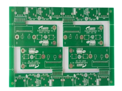
PCB is an important component that connects various electronic parts. Among the many different types of PCBs, 2 layer HAL PCB and multi-layer PCB are the PCBs that many people choose because of their specific applications and advantages. As a company specializing in manufacturing a 2 layer HAL PCB, we will tell you the main […]
The durability and excellent current-carrying capabilities of 4 layer heavy copper PCB stem from their uniform copper thickness, ensuring that uniform copper thickness maintains their benefits and ensures reliable performance and longevity for your application. This guide will explore the steps and techniques for achieving uniform copper thickness for 4-layer heavy copper PCBs. Basics of […]
Among various PCB types, 2 layer TG170 PCBs offer good durability, reliability, and thermal performance. Many buyers ask, “What is the typical lifespan of a 2 layer TG170 PCB?” This guide will answer this question. We will analyze the factors that affect its lifespan, the benefits of using TG170 materials, and the best practices for […]
With the rapid development of the communications industry and data centers, the demand for 400G high-speed PCBs has surged. Achieving high yields in 400G high speed PCB production is critical for manufacturers to meet customer expectations. This guide will explore various methods to improve 400G high-speed PCB production yields. Optimizing 400G high speed PCB manufacturability […]
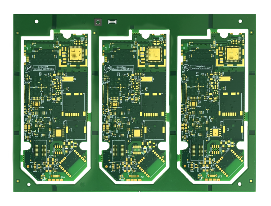
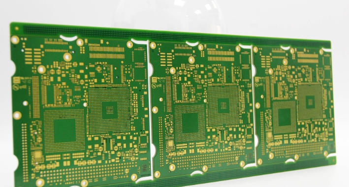
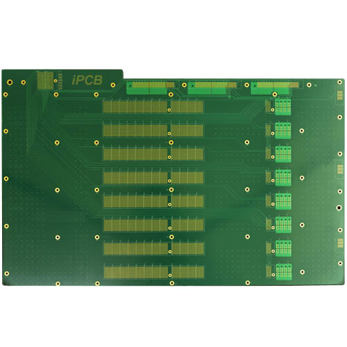
As life improves and the technology of electronic products around us also advances, everyone will pursue higher-performance electronic equipment, followed by the demand for more complex and more adaptable PCBs. Among them, multi-layer PCB have the ability and function to adapt to complex designs. This category has three main types: rigid, flexible, and rigid-flex multilayer […]
Aluminum PCB is a critical PCB component in various electronic applications due to its excellent thermal management properties and durability. However, the costs associated with custom aluminum PCBs can be high for some manufacturers. So, it’s crucial to know how to reduce the associated factors for businesses looking to optimize their budgets without compromising quality. […]
Thermal fatigue is a critical issue in electronic devices using 2 layer heavy copper PCB, affecting PCB performance and longevity. Preventing thermal fatigue is critical for those who manufacture these PCBs. This guide will comprehensively introduce the avoidance of thermal fatigue in 2 layer heavy copper PCBs, highlighting design considerations, material selection, manufacturing processes, and […]
As demand for applications continues to increase, so does the need for high-performance servers that can handle complex workloads. Therefore, manufacturers of various types of servers are constantly seeking innovative solutions to improve efficiency and power density. One solution is to use a 4 layer heavy copper PCB, which offers numerous advantages in terms of […]
PCB technology is constantly evolving, and 400G high-speed PCB is very important for applications requiring high data transmission rates, such as data centers, telecommunications, and advanced computing systems. Customizing these 400G high-speed PCBs can improve performance, meet specific engineering requirements, and provide a competitive advantage. This guide will explain the various customization options available in […]
Among the many designs in PCB design, it is essential to meet customers’ needs for high-current applications while ensuring reliability and efficiency. Then, it is difficult for traditional PCBs to achieve the higher current required by modern electronic devices, leading to problems such as overheating, voltage drops, and signal attenuation. A 4 layer heavy copper […]