Compare different solder mask options for 2 layer 2OZ pcb
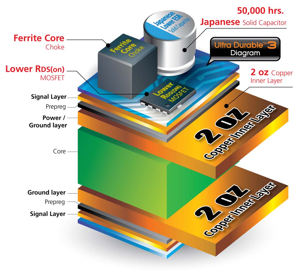
When PCB designers design a 2 layer 2OZ PCB, a pivotal aspect to pay attention to is solder mask selection. In this guide, we’ll look in-depth at solder mask options to give designers the knowledge they need to make informed decisions. Each solder mask option is critical in the performance and reliability of 2-layer 2OZ PCBs, from traditional choices to advanced formulations.
The Traditional Choice of 2 Layer 2OZ PCB
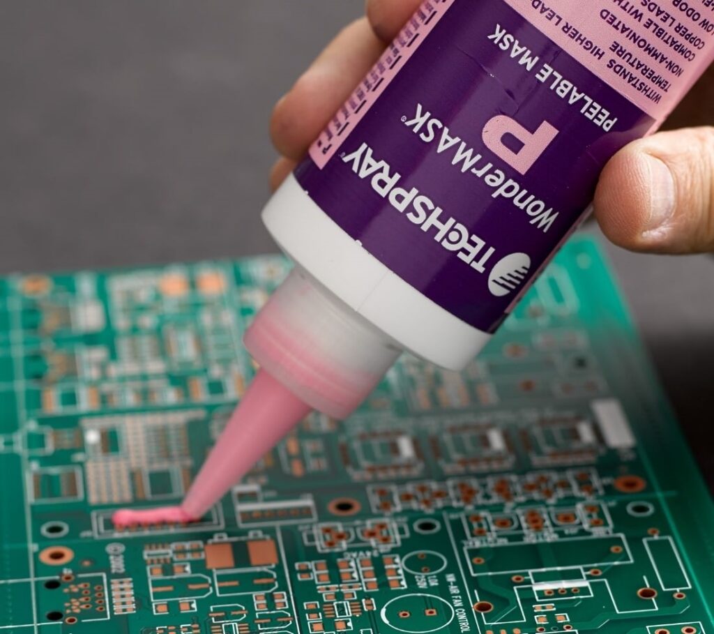
The traditional choices in solder masks are Liquid Photo Imaging (LPI) and Liquid Photo Imaging Solder Mask. LPI solder mask is a common choice in PCB manufacturing and is a protective layer to protect the underlying copper traces from environmental factors and potential damage. It is applied as a liquid photoimaging ink and then exposed to UV through a photomask, hardening the areas that need protection. Unexposed areas are removed during development, leaving a precisely defined and durable mask that protects the copper traces during subsequent assembly and handling.
A layer of liquid photoimaging resistance is used with an LPI solder mask to create circuit patterns on PCBs. The layers are applied similarly, exposed to UV light through a photomask, and developed to form a resist pattern. The resist pattern shields copper during etching, removing unwanted copper and defining desired circuit traces on the PCB. Combining an LPI solder mask and liquid photo-imageable resist layers offers several advantages. It helps define circuit patterns with high precision, ensuring accurate and reliable electrical connections.
UV-curable solder mask
UV curable solder mask is a cutting-edge solution that balances precision and efficiency in manufacturing 2 layer 2OZ PCBs. In PCB production, UV-cured solder mask acts as a protective layer on copper traces, protecting them from environmental factors and potential damage. Unlike traditional Liquid Photo Imaging (LPI) solder masks, UV-curable ones are applied in liquid form and harden rapidly when exposed to UV light. This accelerated curing process significantly reduces production time compared to traditional methods. Using a UV-curable solder mask involves depositing a liquid material onto the PCB surface, spreading it evenly, and then exposing it to UV light through a photomask. Rapid curing reaction creates a durable and precise protective layer. This streamlined process helps improve the efficiency of PCB manufacturing, resulting in faster manufacturing turnaround times.

Thermal Cured Solder Mask Improves Performance of 2 layer 2OZ pcb Designs
Thermoset solder mask is another type in 2 layer 2OZ PCB designs. Thermoset solder mask undergoes a chemical reaction when heated during curing, transforming it into a solid, elastic state. This approach provides a robust protective layer over the PCB’s copper traces, increasing resistance to extreme temperatures, chemicals, and mechanical stress. In manufacturing 2-layer 2OZ PCBs, a thermoset solder mask is applied by depositing it in liquid form onto the board surface. Subsequent exposure to heat triggers the curing process, forming a tough and durable protective layer. Thermoset solder masks are particularly beneficial for enhancing the performance of 2OZ PCB designs. It provides excellent adhesion to substrates, ensuring long-term reliability and preventing delamination.

Impact of Solder Mask Color Options on 2 Layer 2OZ PCB
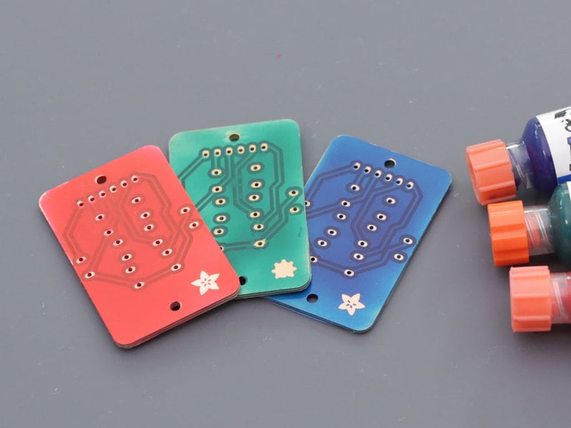
Standard solder mask colors include green, red, blue, black, and white. Traditional green solder masks are still widely used, mainly due to convention and ease of manufacturing. However, different colors may have other effects on the 2 layer 2OZ pcb design and its performance.
For example, green solder masks are often associated with lower manufacturing costs and widespread availability. It is considered a standard option and provides good contrast for component placement and easy viewing of traces during inspection. On the other hand, the red solder mask is known for its high contrast, making it suitable for applications where visual clarity is critical. Blue solder masks are becoming increasingly popular for their aesthetics and increased visibility of white silkscreen marks. The black solder mask has a sleek, modern look while providing good contrast for component identification. White solder mask, although less common, is preferred for LED applications and enhances light reflectivity. Additionally, some colors may have different cure characteristics or exhibit changes in UV light absorption during exposure.
Environmental considerations
A noteworthy option for environmentally friendly solder masks is the use of water-based solder masks. Unlike traditional solvent-based alternatives, water-based solder masks contain fewer volatile VOCs, helping to reduce air pollution during manufacturing. Water-based solder masks are also typically lead-free, complying with global environmental regulations and promoting safer manufacturing practices. Another environmentally friendly option is to choose a solder mask with a lower halogen content. Traditional solder resists may contain halogenated compounds, which may cause environmental concerns due to releasing hazardous substances during disposal or manufacturing. Low-halogen or halogen-free solder masks solve these problems and minimize ecological impact.
Ultimately
Selecting a 2-layer 2OZ PCB solder mask is a critical decision affecting the final product’s aesthetics and functionality. From traditional LPI to advanced formulations, UV curing, thermal curing, etc., all have unique advantages. Hopefully, with this comprehensive guide, our PCB designers can navigate the various solder mask options.

