
FPC PCB Manufacturing Process: From Design to Assembly
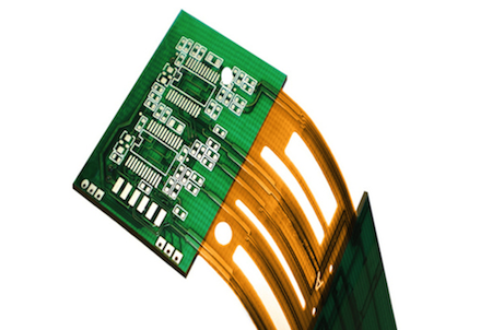
FPC PCB is the backbone of modern electronics, enabling sleek designs and innovative applications. From smartphones to medical devices, these flexible circuits power the technology we rely on daily. But how does an FPC PCB go from a design concept to a fully functional component? This article takes you through the entire FPC PCB manufacturing process, from initial design to final assembly.
Design and Prototyping: Laying the Foundation for FPC PCB Manufacturing
The FPC PCB manufacturing process begins with design. Engineers use specialized software like Altium Designer or Cadence to create a detailed circuit layout, which includes defining the board’s shape, layer stack-up, and component placement.
Designers must consider factors like bend radius, thermal management, and signal integrity. For example, a wearable device might require a highly flexible FPC PCB with a slight bend radius. Once the design is complete, a prototype is created to test functionality and performance. Prototyping helps identify potential issues early, saving time and costs in later stages. It’s a critical step in ensuring the final product meets all specifications.
Material Selection: Choosing the Right Components
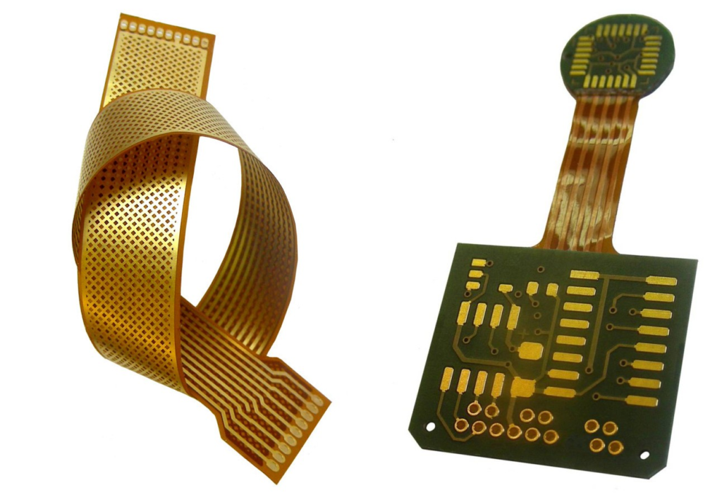
The materials used in FPC PCB manufacturing play a crucial role in performance and durability. The base material is typically polyimide, known for its flexibility and heat resistance. Copper is used for the conductive layers, while adhesives bond the layers together.
Other materials, such as overlays and stiffeners, are added to protect the circuit and provide structural support. For example, a stiffener might be used in areas where components are mounted to prevent bending. Choosing the right materials ensures the FPC PCB can withstand the demands of its intended application, whether it’s a foldable smartphone or a high-temperature industrial device.
Layer Stack-Up and Circuit Patterning
Once the materials are selected, the FPC PCB manufacturing process moves to layer stack-up. This involves arranging the copper and polyimide layers in a specific configuration. The stack-up determines the board’s flexibility, thickness, and electrical performance.
Next, the circuit pattern is transferred onto the copper layers using photolithography. A photoresist is applied to the copper, exposed to UV light through a mask, and then developed to reveal the circuit pattern. The exposed copper is etched away, leaving behind the desired traces. This step requires precision to ensure the circuit functions correctly. Any errors can lead to signal loss or short circuits.
Drilling and Plating: Creating Connections
After patterning, holes are drilled into the FPC PCBs to create vias—connections between layers. These holes are then plated with copper to ensure electrical conductivity.
Laser drilling is often used for high-precision applications, as it can create smaller, more accurate holes. For example, a medical device might require micro-vias to connect densely packed components. Plating strengthens the vias and improves the board’s overall durability. This step is critical for multi-layer FPC PCBs, where interlayer connections are essential.
Coverlay Application: Protecting the Circuit
The next step in the FPC PCB manufacturing process is applying the overlay. This polyimide protective layer shields the circuit from environmental factors like moisture, dust, and mechanical stress.
The overlay is laminated onto the board using heat and pressure. Openings are created for components and connectors, ensuring they remain accessible. A well-applied overlay enhances the FPC PCB’s lifespan and reliability, making it suitable for demanding applications like automotive electronics.
Surface Finish and Component Mounting: Reduce Risk of Error
A surface finish protects the exposed copper and improves solderability. Standard finishes include ENIG (Electroless Nickel Immersion Gold) and HASL (Hot Air Solder Leveling). Each finish has advantages, depending on the application.
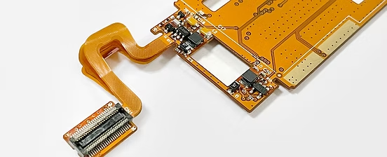
Once the surface finish is applied, components are mounted onto the FPC PCB. This can be done using Surface Mount Technology (SMT) or through-hole mounting. SMT is more common for flexible circuits, allowing for smaller, lighter designs. Automated pick-and-place machines ensure precise component placement, reducing the risk of errors.
Testing and Quality Control: Meeting Industry Standards
Before the FPC PCB is finalized, it undergoes rigorous testing. Electrical tests check for continuity, shorts, and openings, while functional tests ensure the board performs as intended under real-world conditions.
Advanced testing methods, like Automated Optical Inspection (AOI) and X-ray inspection, detect defects that aren’t visible to the naked eye. For example, AOI can identify misaligned components or insufficient solder joints. Quality control ensures the FPC PCBs meet industry standards and customer requirements.
Final Assembly and Packaging: Protecting the FPC PCB
The last step in the FPC PCB manufacturing process is final assembly. This involves integrating the board into the final product, whether a smartphone, a medical device, or an industrial machine.
Once assembled, the FPC PCB is packaged and shipped to the customer. Proper packaging protects the board during transit, ensuring it arrives perfectly.
The Art and Science of FPC PCB Manufacturing
The FPC PCB manufacturing process combines art and science, requiring precision, expertise, and cutting-edge technology. Each step is vital in creating a high-quality, reliable product from design to assembly.
As technology evolves, so will the methods and materials used in FPC PCB manufacturing. By understanding this process, you can make informed decisions and push the boundaries of innovation in your projects.