
From 4-Layer to 8-Layer: Optimizing SSD PCB Stackups for Speed and Durability
Solid-state drives (SSDs) have revolutionized data storage, but their performance hinges on a hidden hero: the printed circuit board (PCB). As SSDs push speed and durability limits, engineers increasingly shift from 4-layer to 8-layer PCB stackups. This evolution isn’t arbitrary—it’s a calculated response to demands for faster data transfer, better heat dissipation, and long-term reliability. Unlike traditional HDDs, SSDs rely on PCBs to manage NAND flash memory, controllers, and power delivery. A poorly designed PCB can bottleneck performance or shorten lifespan. The modern SSD PCB, especially those targeting enterprise or gaming markets, require layered solutions to minimize signal interference and maximize thermal efficiency. Let’s explore why 8-layer stack-ups are becoming the gold standard and how to optimize them for peak results.
HDD vs. SSD PCB Complexity: A Technical Showdown
HDD PCBs are relatively simple, focusing on motor control and basic data routing. In contrast, SSD PCBs resemble miniature supercomputers. They must handle high-speed interfaces like PCIe Gen 5, manage heat from 3D NAND chips, and ensure stable power delivery to power-hungry controllers.
A 4-layer SSD PCB typically includes signal, ground, power, and another signal layer. While cost-effective, this design struggles with crosstalk at speeds above 5 GB/s. Eight-layer stack-ups add dedicated planes for impedance control, shielding, and thermal management. For example, separating analog and digital signals reduces noise, while additional copper layers improve heat distribution.
Why 4-Layer Designs Fall Short for High-Speed SSD PCB Applications
4-layer PCBs work for entry-level SSDs but fail under heavy workloads. Signal integrity degrades as frequencies climb above 2 GHz, causing errors in data transmission. Thermal bottlenecks also emerge—controllers like Phison’s E26 generate up to 10W, which thin 4-layer boards struggle to dissipate.
High-speed SSD PCB design demands precise impedance matching. With only four layers, engineers must compromise between routing density and noise margins. Voltage drop becomes another issue: Limited power planes create instability during peak loads, risking data corruption. Case studies show that 4-layer consumer SSDs experience 15% higher failure rates under sustained writes compared to 8-layer enterprise models.
8-Layer Stackups: Unlocking Speed and Thermal Resilience
Upgrading to 8 layers transforms SSD performance. Engineers gain two critical advantages:
- Enhanced Signal Integrity: Dedicated stripline layers with controlled impedance minimize crosstalk.
- Optimized Thermal Paths: Thicker power planes and thermal vias direct heat away from NAND arrays.
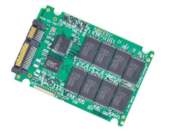
Samsung’s 990 Pro SSD uses an 8-layer design to sustain 7,450 MB/s reads. Its stack includes:
- Layer 1: High-speed signals
- Layers 2/7: Ground planes
- Layers 3/6: Power distribution
- Layer 4: Low-speed control signals
- Layer 5: Thermal diffusion layer
- Layer 8: Shielding
This structure reduces electromagnetic interference (EMI) by 40% compared to 4-layer alternatives.
.png)
Choosing the Best Materials for SSD PCBs
Material selection directly impacts speed and durability. Standard FR-4 works for 4-layer designs but falters in 8-layer high-speed SSD PCB applications. Consider these upgrades:
- Isola I-Speed: Low dielectric loss (Dk=3.37) for PCIe Gen 5 traces
- Rogers 4350B: Superior thermal conductivity (0.69 W/m/K) for power layers
- Panasonic Megatron 6: Tight Dk tolerance (±0.05) for impedance-critical designs
Avoid cost-driven compromises. Inferior materials exacerbate SSD PCB manufacturing defects like delamination or conductive anode filament (CAF) growth. Always specify halogen-free laminates for enterprise SSDs—they withstand 150°C operational temperatures without degrading.
Step-by-Step SSD PCB Signal Integrity Testing
- Pre-Layout Simulation: Use Ansys HFSS to model impedance mismatches.
- Post-Layout Analysis: Measure insertion loss with vector network analyzers (VNA). Target < -3 dB at 10 GHz.
- Eye Diagram Testing: Validate PCIe signal quality—ensure eye height exceeds 100 mV.
- Thermal Cycling: Stress test from -40°C to 125°C to detect warping risks.
Keysight’s Infiniium UXR oscilloscopes excel at catching subtle glitches. For NVMe SSDs, test all lanes simultaneously under 80% load to mimic real-world conditions.
Avoiding Common SSD PCB Manufacturing Defects
Even flawless designs can fail due to production errors. Watch for these pitfalls:
- Microvoids in Plating: Causes impedance spikes. Demand 100% microsection analysis.
- Misaligned Laser Drills: Creates open circuits in HDI vias. Use AOI (automated optical inspection) systems.
- Insufficient Copper Weight: Leads to overheating. Specify 2 oz/ft² copper for power layers.
Partner with fabs that specialize in high-speed SSD PCB design. They’ll enforce tighter tolerances—for example, ±3% impedance control vs. the standard ±10%.
The Future of SSD PCB Innovation
The leap from 4-layer to 8-layer SSD PCBs isn’t just an incremental change—it’s a paradigm shift. As data rates approach 14 GB/s with PCIe Gen 6, layered stacks will become non-negotiable. Emerging trends like liquid crystal polymer (LCP) substrates and embedded graphene cooling layers promise even more significant gains. By mastering stack-up optimization today, engineers can future-proof designs for tomorrow’s storage demands.
Ready to elevate your SSD’s performance? Download Our Free SSD PCB Design Checklist for expert guidelines on layer planning, material selection, and testing protocols.