
From Prototyping to Mass Production: How Double-Sided PCB Save Time and Costs
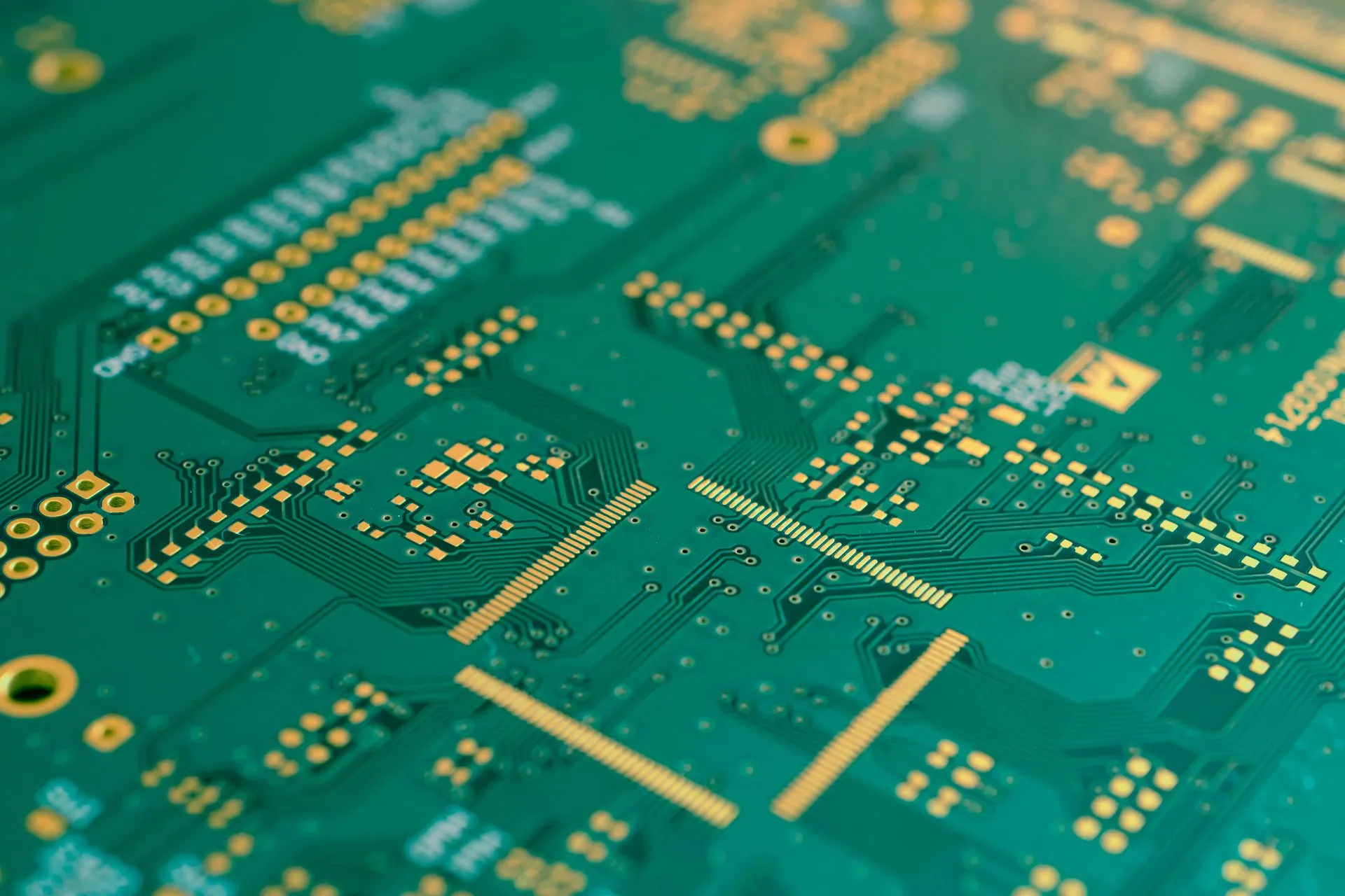
In the fast-paced world of electronics manufacturing, efficiency and cost-effectiveness are critical. Double-sided PCB has emerged as a game-changer, bridging the gap between prototyping and mass production. These versatile circuit boards offer a perfect balance of complexity and simplicity, making them ideal for various applications. This blog post explores how double-sided PCBs streamline the transition from prototyping to mass production, saving time and costs.
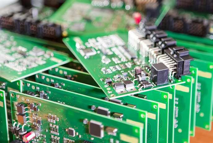
The Role of Double-Sided PCBs in Prototyping
Prototyping is a crucial step in product development. It allows engineers to test designs, identify flaws, and refine functionality before moving to mass production. Double-sided PCB is particularly well-suited for prototyping due to their flexibility and ease of use.
With components mounted on both sides, these boards provide more space for circuitry without increasing the board size. This makes them ideal for testing complex designs. Engineers can quickly iterate on prototypes, reducing development time. The double-sided PCB is also cost-effective, making them a practical choice for early-stage testing. By using double-sided PCB during prototyping, companies can accelerate their development cycles and bring products to market faster.
Streamlining the Transition to Mass Production
Once a design is finalized, transitioning to mass production can be challenging. Double-sided PCBs simplify this process by offering a scalable solution. Their design allows for efficient manufacturing processes, such as automated assembly and surface-mount technology (SMT).
Manufacturers can produce double-sided PCBs in large quantities without significantly changing the production line. This reduces setup time and minimizes costs. The boards’ compatibility with high-speed assembly equipment further enhances production efficiency. Companies can seamlessly transition from prototyping to mass production by using double-sided PCBs, ensuring consistency and quality across all units.
Double-Sided PCB Can Reduce Material Costs
Material costs are a significant factor in electronics manufacturing. Double-sided PCBs help reduce these costs by maximizing the use of board space. With components on both sides, fewer boards are needed to achieve the same functionality.
This efficient use of materials translates to lower production costs. Double-sided PCBs also often require fewer layers than multi-layer boards, reducing material expenses. For example, a study by the IPC found that double-sided PCBs can reduce material costs by up to 30% compared to multi-layer alternatives. Double-sided PCBs offer a cost-effective prototyping and mass-production solution by minimizing material waste.
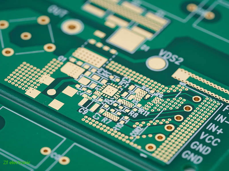
Double-Sided PCB Can Enhance Design Flexibility
Design flexibility is essential for creating innovative products. Double-sided PCBs provide engineers with more options for component placement and routing. This flexibility allows for more compact and efficient designs.
For instance, high-density designs can benefit from the additional space provided by double-sided PCBs. Engineers can place components on both sides, reducing the overall board size. This is particularly useful for consumer electronics, where space is often limited. The ability to experiment with different layouts during prototyping ensures that the final design is optimized for mass production. This flexibility saves time and reduces the risk of costly design changes later in the process.
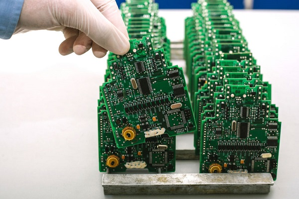
Improving Manufacturing Efficiency
Manufacturing efficiency is critical for meeting production deadlines and controlling costs. Double-sided PCBs are compatible with automated assembly processes, which significantly improve efficiency.
Automated pick-and-place machines can quickly populate components on both sides of the board. This reduces assembly time and minimizes human error. Additionally, double-sided PCBs can be inspected and tested using automated systems, ensuring high-quality output. By leveraging these manufacturing advantages, companies can produce double-sided PCBs at scale without compromising quality or speed.
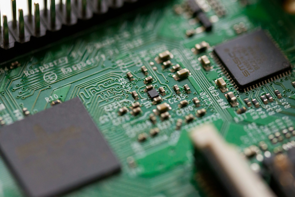
Ensuring Reliability and Durability
Reliability is a top priority in electronics manufacturing. Double-sided PCBs are known for their durability and performance. Through-hole technology and vias ensure strong connections between layers, enhancing the board’s reliability.
These boards are also less prone to signal interference, making them suitable for high-frequency applications. For example, double-sided PCBs are commonly used in telecommunications and automotive electronics, where reliability is critical. Manufacturers can deliver products that meet the highest quality and durability standards by choosing double-sided PCBs.
Supporting Sustainable Manufacturing
Sustainability is becoming increasingly important in electronics manufacturing. Double-sided PCBs contribute to sustainable practices by reducing material waste and energy consumption.
The efficient use of board space minimizes the amount of raw materials needed. Additionally, the streamlined manufacturing process reduces energy usage. For instance, double-sided PCBs require fewer steps than multi-layer boards, lowering the overall carbon footprint. Companies can align with sustainability goals by adopting double-sided PCBs while maintaining cost-effectiveness.
The Advantages of Double-Sided PCB
From prototyping to mass production, double-sided PCBs offer numerous advantages. They streamline the development process, reduce costs, and enhance design flexibility. Their compatibility with automated manufacturing ensures efficiency and reliability. Companies can accelerate product development, improve quality, and support sustainable practices by choosing double-sided PCBs. Whether designing a new product or scaling up production, these boards provide a practical and cost-effective solution.