
Gold Finger PCB Beveling: Importance and Process Explained
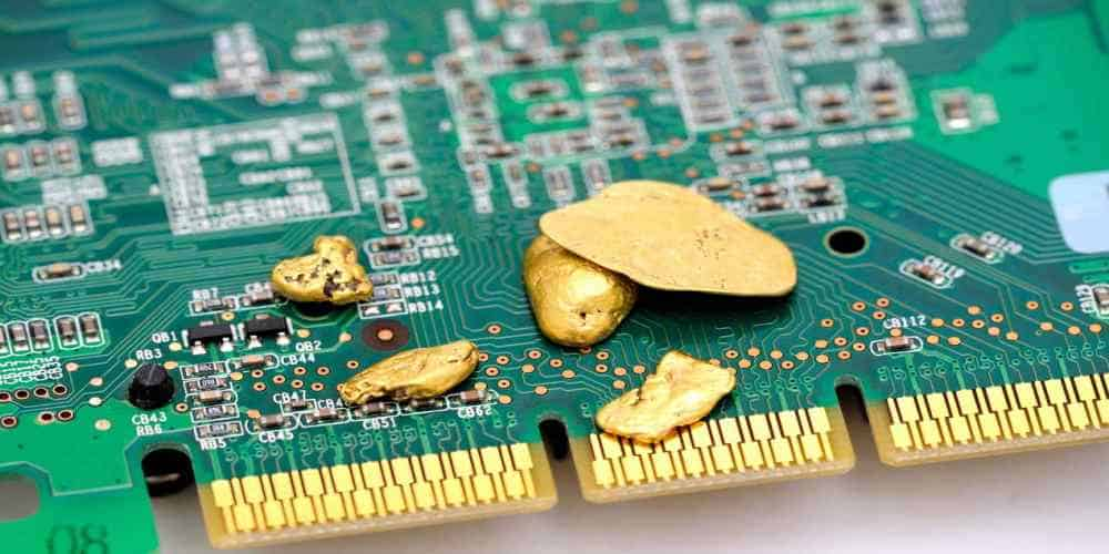
Gold finger PCBS are essential for high-speed and high-reliability electronic applications. In 2025, as edge connectors become more precise and demanding, beveling these gold fingers has grown from a niche process into a design standard. Why? Because poorly bevelled PCBS risk mechanical failure, connection instability, and costly replacements. Beveling creates a smooth, angled edge at the contact interface, improving both insertion performance and the connector’s lifespan. Whether you’re producing boards for servers, data centres, or gaming rigs, ignoring the bevel is a rookie mistake. This article dives deep into the process and significance of gold finger PCB beveling—what it is, why it’s crucial, and how to get it right.
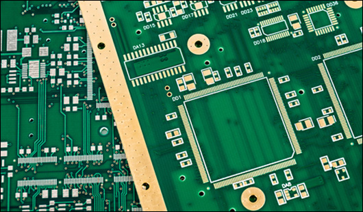
What Is Gold Finger PCB Beveling and Where Does It Apply
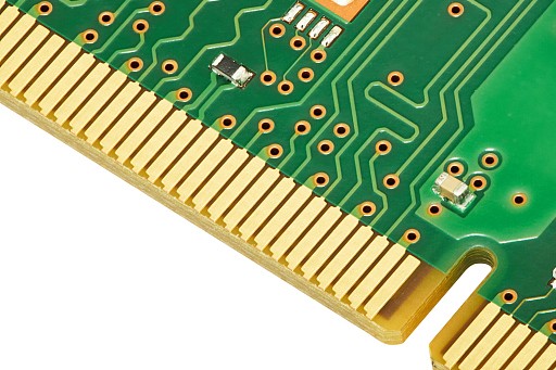
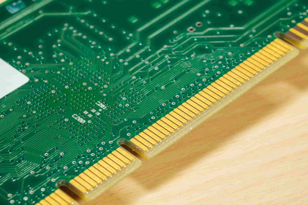
PCB beveling refers to the machining of the board edge to form a precise angle, typically 30° or 45°, on gold-plated contact pads. This edge refinement reduces the insertion force, preventing damage to the connector. Though it may seem like a minute is just an adjustment moment, it’s essential in designs with frequent mating cycles. Industries like telecom, aerospace, and industrial computing widely apply this technique. Notably, gold finger PCBS without proper beveling can experience abrasion and misalignment over time. Beveling ensures a reliable interface, minimising both physical wear and signal interference. Without it, even top-tier won’t save a connector from eventually breaking down.
The Mechanical Benefits of Beveling
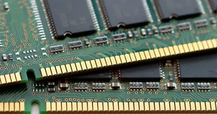
Beveling reduces friction during insertion and extraction cycles. The angled edge guides the connector into its socket, aligning it more smoothly and reducing mechanical stress. This isn’t just about ease of use; it prevents edge chipping and delamination under force. For multi-layer PCBS, beveling also helps avoid stress fractures that often develop near sharp corners. Additionally, the consistent contact pressure provided by bevelled edges boosts signal stability. A flat-cut PCB may look fine on paper, but in real-world applications, it fails to perform under repeated cycles. Mechanical efficiency, after all, is where reliability starts.
Electrical Performance and Signal Integrity
Gold finger PCB beveling directly impacts electrical performance. The smoother the connection, the lower the contact resistance. Beveling eliminates micro-gaps that would otherwise interfere with signal flow. Especially in high-frequency applications, even minor inconsistencies can cause reflections or attenuation. Bevelled gold fingers maintain stable conductivity over time, which is critical in devices where speed and accuracy are non-negotiable. Additionally, less physical stress means a lower risk of micro-cracking in the gold plating—something that can dramatically affect signal quality. That extra five degrees of angle might seem trivial, but in the world of data transmission, it’s everything.
Manufacturing the Perfect Bevel
Creating the perfect bevel requires specialised CNC equipment and tight process control. After the main PCB structure is fabricated and gold plated, the beveling step comes last. Manufacturers use dedicated routing bits to create uniform angles without damaging adjacent layers. Any slip-up here can compromise the entire board. Tolerances are tight—typically ±5 degrees—and require constant quality monitoring. For OEMS and designers, working with endorsed manufacturers is key. You don’t want your gold finger PCB ruined by a rushed beveling job. Instead, demand quality checks, bevel-depth measurements, and consistency in angle across every production batch.
Common Beveling Mistakes in Gold Finger PCB Manufacturing
One of the most common mistakes is beveling after final inspection. This can expose sensitive layers or leave edges unprotected. Another issue is poor angle consistency, which leads to uneven connector pressure. Then there’s under-beveling, where the angle is too shallow to reduce insertion force. The best prevention? Work with a fabricator that specialises in gold finger PCBS and provides clear beveling standards. Ensure your design files specify bevel angles and that your partner uses automated beveling tools. Skipping these steps risks high RMA rates and doesn’t make it happen—it’s built into the process.
Choosing the Right Angle for Your Application
Not all applications need the same bevel. A 30° bevel suits most commercial devices, but rugged environments—think automotive or aerospace—often benefit from a 45° edge. Why? The steeper angle can withstand more insertion pressure and provides a better fit. It’s heavy-duty connectors. It’s also about user handling. Thicker boards need deeper bevels to maintain the same surface taper. And with custom designs becoming more common in 2025, angle flexibility matters more than ever. Designers should consult manufacturers early in the process. This ensures the bevel supports both the mechanical and electrical goals of the project.
Compliance and Standards
Bevelinit’sn’t just a best practice—it’s a requirement in many cases. IPC-A-600 and IPC-2221 both mention guidelines for gold finger preparation, including beveling. In regulated industries, failure to meet these can block product approvals or certifications. Moreover, standards like UL 796 also reference mechanical edge treatment. For B2B buyers, showing compliance helps close deals faster. For contract manufacturers, sticking to these guidelines reduces liability and risk. Staying compliant is not just about ticking boxes—it’s a competitive advantage. A properly bevelled gold finger, Pyou’rels partners and clients, you’re not cutting corners.
Investing in Gold Finger PCB Beveling for Long-Term Reliability
In 2025, performance and reliability expectations are higher than ever. A well-designed gold finger PCB with proper beveling can be the difference between a product that lasts and one that fails in the field. From smoother mechanical insertion to more stable signal transmission, bit-sing is no longer optional—it’s foundational. Manufacturers and designers alike must prioritise this step to meet today’s quality standards in the tech landscape. With the right equipment, partners, and processes, beveling becomes a strategic asset, not a checklist item. Don’t underestimate the edge—literally. Make beveling part of your PCB success strategy.