How are components mounted on both sides of a Double Sided PCB?
Double sided PCB, a cornerstone of modern electronics, offer unparalleled flexibility and efficiency in circuit design. By allowing components to be mounted on both sides, these PCBs maximize space and enhance the device’s overall functionality. This blog post will delve into the mounting processes, techniques, and benefits of Double Sided PCBs, equipping you with the knowledge to make informed design decisions.
Understanding the Basics of a Double Sided PCB
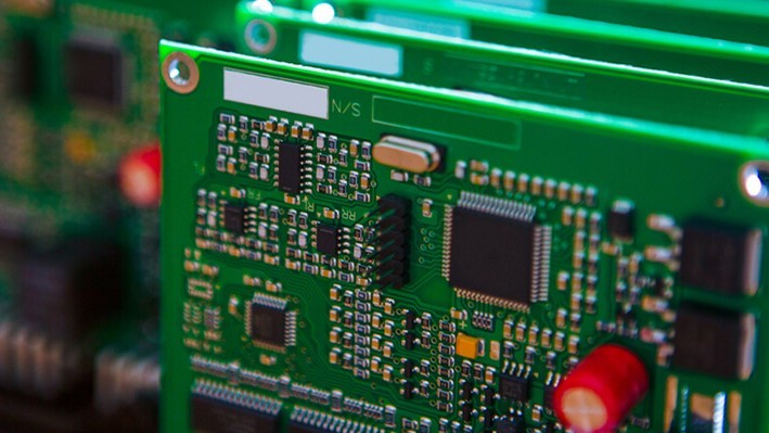
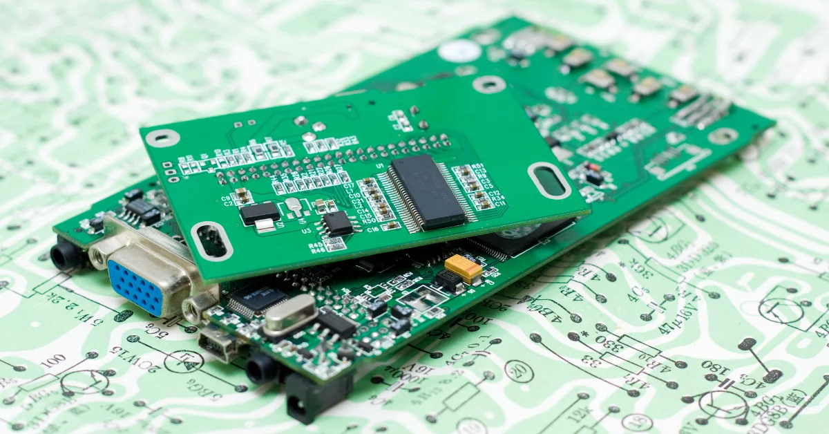
Before we delve into how components are mounted, it’s essential to understand what a Double Sided PCB is and how it differs from a single-sided PCB. A Double Sided PCB is a circuit board that has copper conductive layers on both the top and bottom sides. These layers are connected via vias, which are small holes that allow electrical signals to pass between the two sides. This design significantly increases the space for components and connections, making it a top choice for more complex circuits.
Double sided PCBs, with components spread across both surfaces, represent a more intricate design potential. Their complexity in manufacturing, necessitating additional processes like precise alignment and through-hole plating, underscores the expertise required in their production.

Several Key Steps to Mounting Components
Mounting components on a Double Sided PCB involves several key steps to ensure the components are securely placed and properly connected. Soldering is the most common method for mounting components on both sides of a Double Sided PCB. The board is usually coated with a layer of solder paste, which helps hold the components during assembly. With through-hole components, the leads of the component are inserted into pre-drilled holes in the PCB, and the board is then passed through a reflow oven to melt the solder paste and secure the component. Surface mount components (SMDs) are placed on the PCB surface and secured with solder paste.
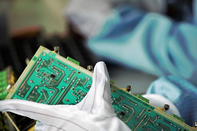
With Double Sided PCBs, careful handling is required to ensure that components on one side do not interfere with components on the other side. The board is mounted on a jig or fixture to hold it while each side is processed separately. This allows components to be mounted on the top and then on the bottom using a combination of reflow, wave soldering, or manual soldering techniques.
Types of Components Mounted on Double Sided PCBs
Double sided PCBs can accommodate a variety of components, each serving a distinct function within the circuit. These include resistors, capacitors, diodes, transistors, inductors, connectors, and more complex components like integrated circuits (ICs), microprocessors, and sensors, providing a comprehensive understanding of their functionality.
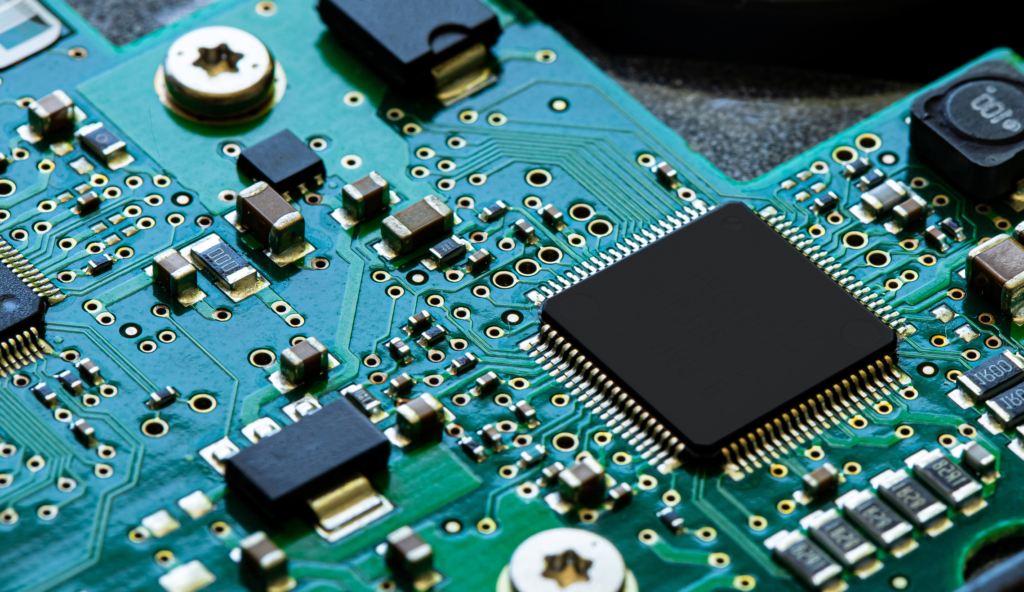
Surface-mount components (SMDs): These are the most commonly used components on Double Sided PCBs because they can be mounted directly onto the board’s surface without needing holes. SMDs, such as chip resistors, capacitors, and ICs, come in various shapes and sizes.
Through-hole components: These are components with leads that are inserted into holes drilled into the PCB and then soldered to the board. Common through-hole components include connectors, large capacitors, and power components.
The ability to mount both SMDs and through-hole components on a Double Sided PCB makes it a versatile option for circuit designers. Placing through-hole components on one side and SMDs on the other maximizes space for efficient, compact circuit layouts. This versatility makes Double Sided PCBs ideal for complex designs requiring numerous components.

Challenges in the Component Mounting Process
While double-sided PCBs offer numerous advantages, mounting components on both sides presents some challenges. One of the main challenges is alignment.
Careful alignment is crucial when mounting components on both sides to prevent interference and ensure correct electrical connections. Misalignment can lead to short circuits, broken connections, or component failure. A challenge is precise soldering, especially with multi-layer boards and closely spaced or overlapping components. Knowing these challenges will help you prepare for potential difficulties in your design process.
In addition, the through-hole technology used in Double Sided PCBs must be carefully managed. Through-holes are small holes that connect the copper layers on both sides of the PCB and must be precisely drilled and plated to ensure a reliable electrical connection. Poor through-hole quality can lead to electrical shorts, signal degradation, and complete circuit failure.
Reflow and Wave Soldering Technology
Reflow and wave soldering are commonly used for mounting components on Double Sided PCBs. Both methods have advantages and are often used to produce high-quality, reliable PCBs.
Reflow is the most common soldering technique for surface-mount components (SMDs). The process begins by applying solder paste to the desired locations on the PCB. The components are then placed on the solder paste, and the PCB passes through a reflow oven. The heat from the oven melts the solder paste, securing the components to the board. Reflow is particularly useful for Double Sided PCBs because it can efficiently mount SMDs on both sides of the board.
Wave soldering technology is often used for through-hole components. In wave soldering, molten solder flows through PCB holes to connect components, leading to copper pads. For Double Sided PCBs, wave soldering is usually used on one side of the board, while reflow soldering is used on the other.

The Benefits of Using Double Sided PCBs
The primary benefit of Double Sided PCBs lies in their ability to maximize available space, a crucial factor in creating compact, efficient circuits. This is particularly significant in applications where size and weight are critical, such as mobile devices, wearables, and automotive electronics, underlining their practical applications.
In addition to saving space, Double Sided PCBs also improve signal routing. By routing signals on both sides of the board, engineers can avoid the need for complex and expensive multilayer boards. This leads to lower manufacturing costs while maintaining high-performance standards. The increased number of available connections also improves the overall performance and reliability of the circuit.
Another benefit is that Double Sided PCBs offer better heat dissipation. Since components are mounted on both sides of the board, heat can be more evenly distributed, reducing the risk of overheating. This is particularly important in high-power applications or devices that generate significant amounts of heat during operation.
The Future of Double Sided PCBs
Double sided PCBs are an indispensable tool for modern electronic devices, offering significant space utilization, performance, and flexibility advantages. Mounting components on both sides of a board enables designers to create more compact, efficient, and reliable circuits. As electronic devices become smaller and more complex, demand for Double Sided PCBs is expected to grow. Their versatility and advances in manufacturing processes will continue to play a key role in driving innovation across a wide range of industries, from consumer electronics to automotive and aerospace.

