
How do 400G high speed PCB handle high-frequency signals?
In the field of high-performance computing and data transmission, 400G high speed PCB play a crucial role in managing the complexity of high-frequency signals. These advanced printed circuit boards are designed to accommodate the higher data rates and lower signal integrity challenges associated with 400G Ethernet and other high speed applications. In this blog post, we will take a deep dive into how 400G high speed PCBs handle high-frequency signals and discuss the key factors that affect their performance and reliability.
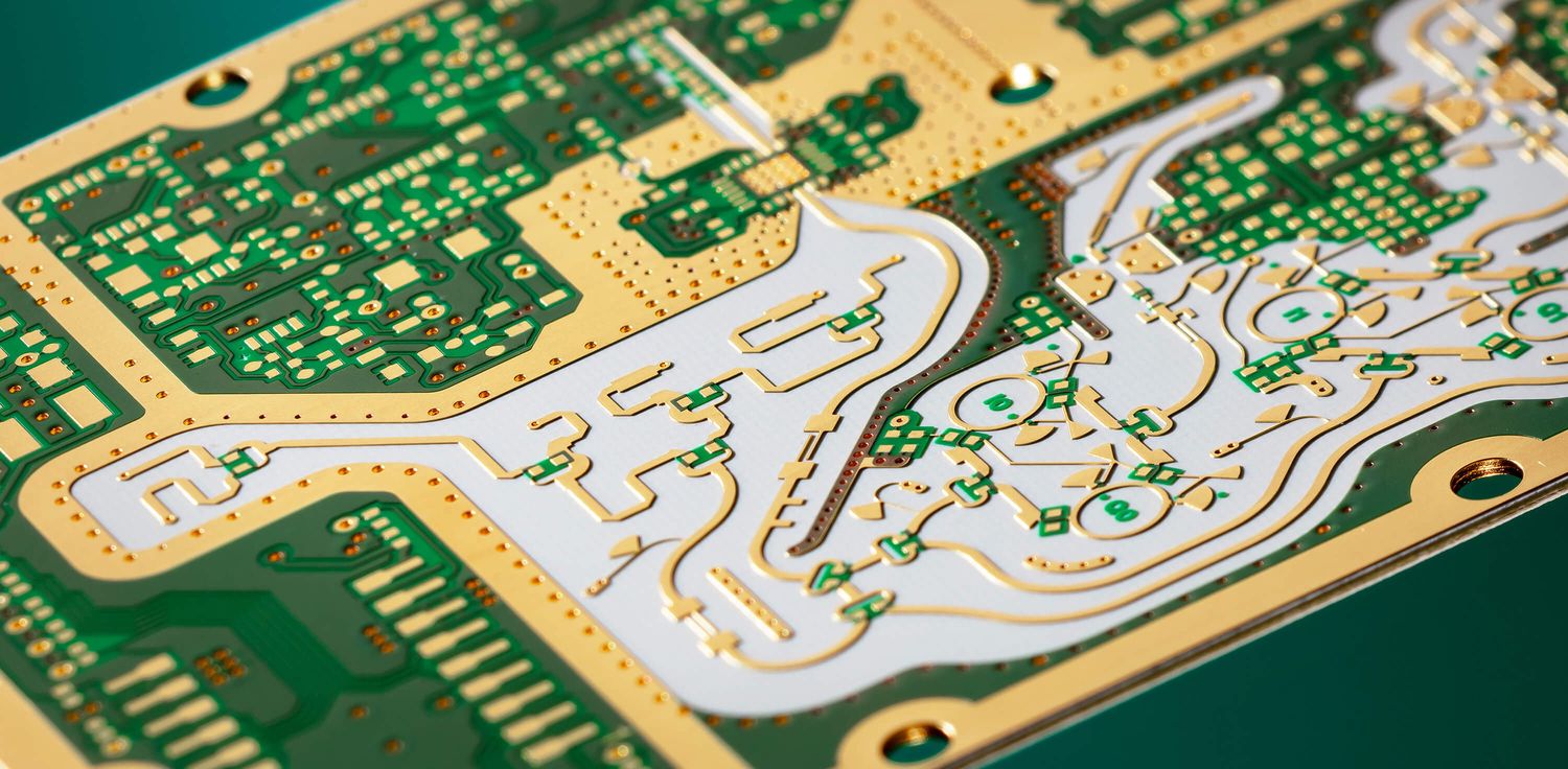
Understanding the Design of 400G high speed PCB
400G high speed PCBs are designed to manage data transmission rates of up to 400 gigabits per second. This requires meticulous attention to design and material selection as well as advanced manufacturing techniques. The main challenge of 400G high speed PCB design is to minimize signal loss and distortion while maintaining the integrity of high-frequency signals.
High-frequency signals are prone to problems such as signal attenuation, crosstalk, and electromagnetic interference. To mitigate these challenges, 400G high speed PCBs are designed with specialized materials with low dielectric loss and often include features such as controlled impedance and differential signalling. These design elements help maintain signal integrity and reduce the risk of data errors.
Material Selection for Optimal Signal Integrity
One of the most critical aspects of designing 400G high speed PCBs is the choice of materials. The substrate material must have specific electrical properties, such as low dielectric constant and low dissipation factor, to support high-frequency signal transmission. Manufacturers commonly use FR-4 in 400G high speed PCBs, but they prefer more advanced materials for superior performance.
These materials help reduce signal loss and maintain the required impedance level. They also help improve the PCB’s thermal stability, which is critical for maintaining high-frequency signal integrity. Choosing the suitable material is a delicate balance between performance and cost, as higher-quality materials are usually expensive.
The Role of Controlled Impedance in 400G high speed PCB
Controlled impedance is an essential requirement for 400G high speed PCBs. It refers to the precise adjustment of the electrical impedance of the signal traces on the PCB, which is critical to minimize signal reflections and maintain signal quality. In high-frequency applications, even slight deviations in impedance can cause severe signal attenuation.
To achieve controlled impedance, designers must carefully calculate the width, spacing, and layer structure of PCB traces. This process often involves using advanced simulation software to simulate signal behaviour and optimize trace layout. Properly controlled impedance ensures that 400G high speed PCBs can handle high data rates without introducing excessive signal distortion or loss.
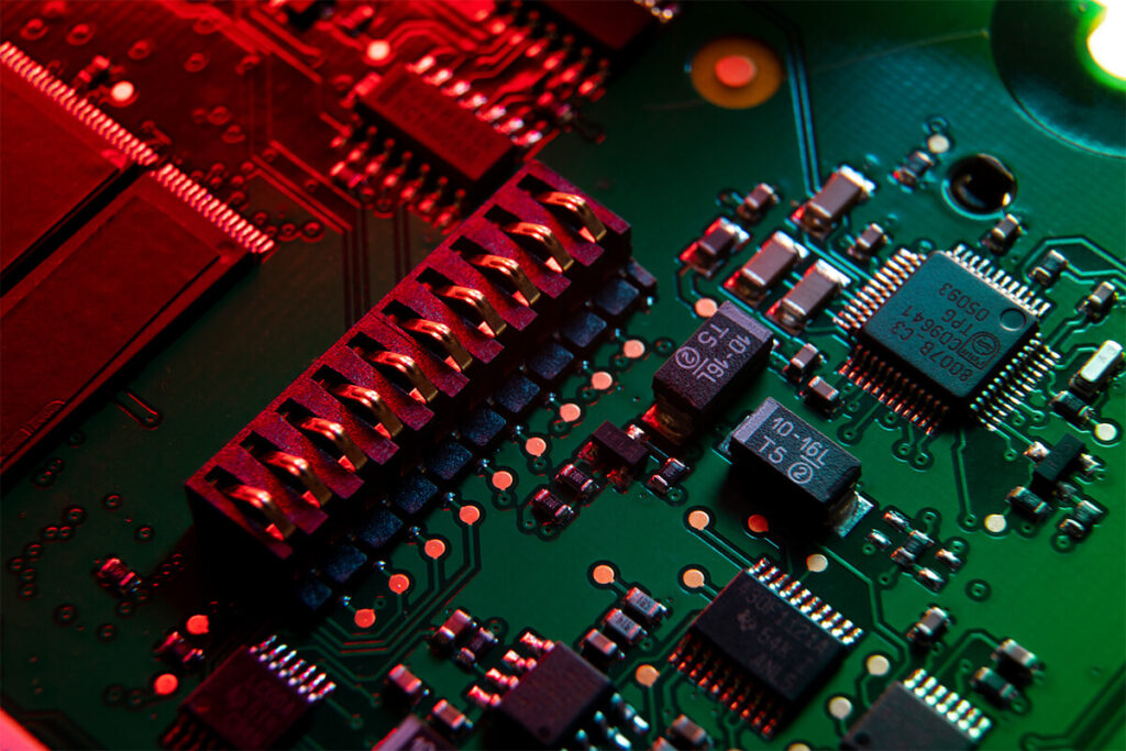
Solving Signal Integrity Challenges in High-Frequency Applications
Signal integrity is a significant concern for 400G high speed PCBs because high-frequency signals are more susceptible to degradation. Factors such as trace length, signal routing, and via design all play a role in maintaining signal quality. For example, longer trace lengths increase signal attenuation, while poorly designed vias introduce unwanted parasitic capacitance and inductance.
To address these challenges, designers often use techniques such as differential signalling and microstrip or stripline configurations. Differential signalling involves using pairs of traces to transmit anti-phase signals, which helps cancel noise and reduce EMI. Microstrip and stripline configurations, on the other hand, provide better impedance control and reduce signal loss by routing within PCB layers.
The impact of crosstalk and EMI on it
Crosstalk and electromagnetic interference are two critical issues that can affect the performance of 400G high speed PCBs. Crosstalk occurs when signals in adjacent traces interfere with each other, resulting in signal distortion and data errors. External electromagnetic fields cause EMI, which can disrupt the PCB’s operation.
To mitigate crosstalk, designers must carefully manage the spacing between signal traces and isolate sensitive areas using ground planes. Shielding techniques also help reduce the effects of EMI. Proper PCB layout and design practices are essential to minimize these issues and ensure the reliable operation of 400G high speed PCBs.

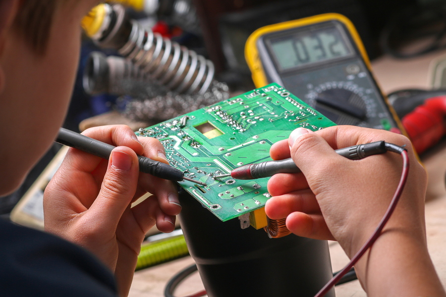
Advanced Testing and Verification Techniques for 400G high speed PCB
Given the complexity of 400G high speed PCBs, rigorous testing and verification are required to ensure they meet performance standards. Testing typically involves measuring parameters such as insertion loss, return loss, and signal-to-noise ratio. These tests help identify potential issues and verify that the PCB can handle high-frequency signals without performance degradation.
Advanced testing techniques, such as time-domain reflectometry and vector network analysis, are often used to analyze PCBs’ signal behaviour and impedance characteristics. These methods provide detailed insights into PCB performance and help designers fine-tune their designs to meet the stringent requirements of 400G applications.
Future technology trends and innovations
As data demands continue to grow, the need for higher-speed PCBs is becoming increasingly evident. The next generation of high speed PCBs is likely to go beyond 400G, requiring more complex materials and design techniques. Experts expect innovations like advanced signal processing algorithms, new PCB materials, and improved manufacturing processes to play an essential role in developing future high-speed PCBs.
In addition, the integration of optical interconnects and advanced packaging technologies may further enhance the performance and scalability of 400G high speed PCBs. These advances are critical to supporting the next wave of data-intensive applications, from cloud computing and artificial intelligence to 5G networks and beyond.
400G high speed PCB Enable high speed Data Transmission
400G high speed PCBs are at the forefront of modern technology, enabling the high speed data transmission required for a wide range of applications. By carefully managing high-frequency signals through advanced design, material selection, and testing techniques, these PCBs ensure reliable performance and signal integrity.