How Do Double-Layer PCB Improve Circuit Performance and Reduce Size?
As demand for smaller, more efficient electronic devices grows, engineers face the challenge of increasing circuit performance while reducing size. Double-layer PCB solves this problem by providing a more efficient design that leverages the power of two conductive layers to improve circuit functionality and optimize space. These PCBs are fundamental to telecommunications, consumer electronics, automotive systems, and medical device applications, where performance and compactness are critical. In this blog, we’ll dive into the specific ways that Double-layer PCBs improve circuit performance and reduce the overall size of a device.
Improved Signal Integrity and Faster Data Transmission with Double Layer PCB
One of the primary benefits of Double-Layer PCBs is their ability to enhance signal integrity. By utilizing two layers of conductive material, engineers can create shorter and more efficient signal pathways essential for high-speed data transmission. Compared to single-layer PCBs, Double-Layer PCBs offer better routing options, allowing high-frequency signals to travel with minimal distortion and attenuation.
A key study published in IEEE Transactions on Components, Packaging, and Manufacturing Technology in 2020 found that Double-layer PCBs reduce signal degradation by up to 30% in high-speed data transmission applications. This improvement is particularly valuable in modern electronics, where devices like smartphones, gaming consoles, and networking equipment require high-speed data communication with minimal loss or interference. For example, high-performance consumer electronics like Apple’s iPhone rely on double-layer PCBs to ensure the smooth operation of processors and memory modules. These PCBs allow manufacturers to reduce signal loss, providing faster data processing and improved performance in devices with increasingly complex features.

Compact Circuit Designs with double-layer PCB
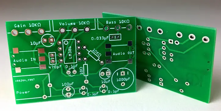
Miniaturization is a key driver in the electronics industry, and double-layer PCB is at the forefront of this trend. These PCBs provide an additional conductive layer, allowing for more compact and efficient circuit designs. Using both sides of the PCB for routing traces means that engineers can fit more components into a smaller footprint, reducing the overall size of electronic devices.
A great example of miniaturization through double-layer PCBs is in wearable devices such as smartwatches. Companies like Samsung and Fitbit have incorporated double-layer PCBs into their designs to create smaller, more efficient devices without sacrificing performance. A report by Digi-Key in 2021 found that the trend toward compact, multi-layer PCB designs has enabled manufacturers to reduce the size of wearables by up to 50% while maintaining or even improving their
Enhanced Power Efficiency and Distribution
Another essential benefit of double-layer PCBs is their ability to improve power distribution and energy efficiency. Effective power management is critical to optimizing performance and preventing overheating in high-power applications such as electric vehicles, power supplies, and industrial machinery. Double-layer PCBs help distribute power more efficiently by providing dedicated layers for power and ground planes.
Double-layer PCBs can reduce the potential for power loss and improve thermal management by using separate power and ground planes. In the automotive industry, double-layer PCBs are used in power control units for electric vehicles (EVs). They can improve the efficiency of power distribution in electric cars by up to 25%, significantly reducing the risk of overheating in high-voltage battery systems. Power efficiency is also critical in medical devices such as pacemakers and insulin pumps.

Noise Reduction and Electromagnetic Interference Control
Electromagnetic interference (EMI) is a significant concern in modern electronics, especially in high-speed circuits and sensitive applications. Double-layer PCBs offer substantial advantages in controlling EMI and minimizing crosstalk between adjacent traces. Including a dedicated ground plane on one of the layers helps shield sensitive signals from external interference, ensuring cleaner and more reliable performance.
A study published in Electronics Design in 2020 demonstrated that double-layer PCBs could reduce crosstalk by up to 40% compared to single-layer designs. This reduction in interference is particularly valuable in high-frequency applications such as wireless communication systems, where maintaining a clear signal is critical for optimal performance.
Cost-Effectiveness in Mass Production
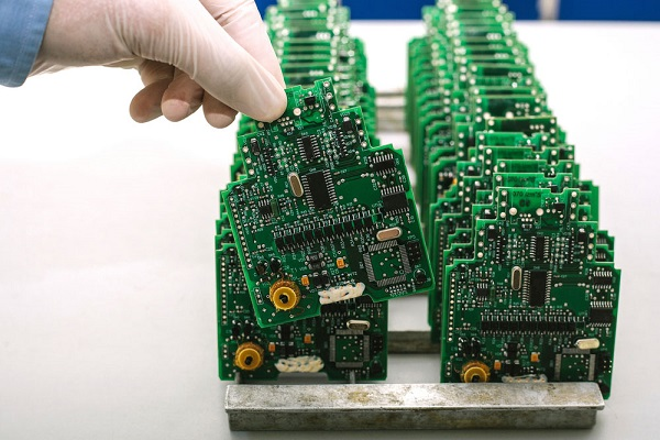
While Double-Layer PCBs may have a higher upfront cost compared to single-layer designs, they offer long-term cost savings, especially in high-volume manufacturing. By allowing manufacturers to integrate more components into a smaller board, Double-Layer PCBs help reduce material costs and improve production efficiency. The PCB’s smaller size also means fewer components and boards are needed to achieve the same functionality, reducing overall production expenses.
A 2021 study by McKinsey & Company found that the cost of producing double-layer PCBs in high-volume runs decreases significantly, reducing per-unit costs for mass-produced devices. This cost efficiency is particularly beneficial in industries like consumer electronics, where manufacturers strive to keep device prices competitive without compromising quality.
For example, companies like Apple and Samsung produce millions of smartphones yearly, and using Double-Layer PCBs allows them to reduce costs while meeting performance requirements. By integrating more components into a smaller space, these companies can create sleek, feature-rich devices that appeal to consumers while keeping production costs in check.

Design Flexibility and Innovation with Double Layer PCBs
One key advantage of Double-Layer PCBs is the design flexibility they offer. Using both sides of the PCB for routing traces allows engineers to experiment with more complex circuit layouts, leading to innovative designs that push the boundaries of what is possible in electronics.
This design flexibility is particularly important in industries like aerospace, automotive, and medical devices, where reliability and performance are critical. Double-layer PCBs allow engineers to integrate multiple functions into a single compact board, creating cutting-edge products that meet stringent performance, size, and weight requirements.
For instance, in the automotive industry, Double-Layer PCB is used to design more efficient and compact control systems for electric vehicles. As the demand for electric cars continues to rise, Double-Layer PCBs are helping manufacturers meet the challenges of designing smaller, more efficient, and more reliable electronic systems.
Choose Double-Layer PCB for Your Electronics
Double-layer PCBs offer a wide range of benefits that significantly improve circuit performance while reducing the size of electronic devices. These PCBs are indispensable in modern electronics, from enhanced signal integrity and reduced noise to better power distribution and design flexibility. By leveraging the advantages of double-layer PCBs, manufacturers can create high-performance, compact devices that meet the demands of the modern consumer while ensuring long-term cost efficiency and product reliability.

