
How do mid low loss PCB perform in applications with high data rates?
The mid low loss PCB is a critical component in modern electronics, especially for applications that require high data rates. As technology advances, the demand for PCBs that can efficiently handle these high-speed signals without compromising performance continues to grow. This blog post will examine the performance of mid low loss PCBs in high-data-rate applications.
Understanding Mid low loss PCB
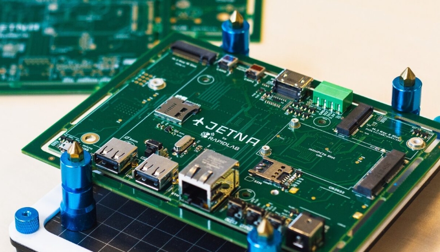
Mid low loss PCBs are designed to reduce signal loss during transmission, which is critical in high-frequency and high-speed applications. Unlike traditional PCBs, mid low loss PCBs use materials with lower dielectric loss, thereby minimizing signal attenuation and improving overall performance. These PCBs are often used in applications where maintaining signal integrity is critical, such as telecommunications, data centres, and high-speed computing.
The main benefit of mid low loss PCBs is their ability to maintain signal strength over long distances and in complex circuit designs. By reducing dielectric loss, these PCBs enable faster data transmission with minimal attenuation, ensuring high data rates without compromising signal quality. For industries that rely on accurate and rapid data transmission, such as networking and telecommunications, mid low loss PCBs are an indispensable solution.
Key Features in High Data Rate Applications
Mid low loss PCBs have specific features that make them suitable for high data rate applications. One key feature is the use of advanced dielectric materials with low dissipation factors. These materials minimize signal loss, ensuring the transmission of high-frequency signals with minimal distortion. In addition, mid low loss PCBs often employ optimized trace geometry and controlled impedance to enhance signal integrity further.
Another essential feature is the use of high-quality copper with low surface roughness. This reduces signal reflections and losses, which is especially important at high frequencies. The combination of these features enables mid low loss PCBs to support data rates exceeding several gigabits per second, making them ideal for applications such as 5G communication networks, high-speed interconnects, and broadband signal processing.
Benefits of Using Loss PCBs in High-Speed Applications
One of the main benefits of using mid low loss PCBs in high-speed applications is their ability to maintain signal integrity over long distances. In high-frequency environments, signal loss and distortion can severely impact performance. Mid low loss PCBs mitigate these issues by reducing dielectric losses and ensuring that signals remain strong and clear even when traversing complex circuit paths.
Additionally, mid low loss PCBs enable designers to achieve higher data rates without excessive power consumption. This is because less signal amplification is required to compensate for losses, resulting in more efficient and reliable operation. In addition, the enhanced performance of mid low loss PCBs reduces the likelihood of errors and data corruption, which is critical in applications where accuracy and speed are crucial.
Applications in High Data Rate Environments
Mid low loss PCBs are widely used in applications that require high data rates and low signal attenuation. In the telecommunications sector, these PCBs are integral to the development of high-speed communication networks, including 5G and fibre optic systems. The ability to quickly and accurately transmit large amounts of data is critical in these applications, and mid low loss PCBs provide the necessary performance characteristics to meet these needs.
Data centers use mid low loss PCB in high-speed interconnects and server architectures where maintaining signal integrity is essential for efficient data processing and transmission. Mid low loss materials ensure minimal signal loss between components, supporting the high data throughput required in these environments. Other applications include high-speed computing, automotive electronics, and advanced radar systems, where the ability to handle high data rates is an essential requirement.
Challenges in Design and Manufacturing
Developing and manufacturing mid low loss PCBs for high-data-rate applications presents several challenges. One of the main difficulties is selecting suitable materials with low dielectric loss and mechanical stability. Engineers must carefully choose these materials to balance performance and cost, as high-performance options can be expensive and challenging to work with.
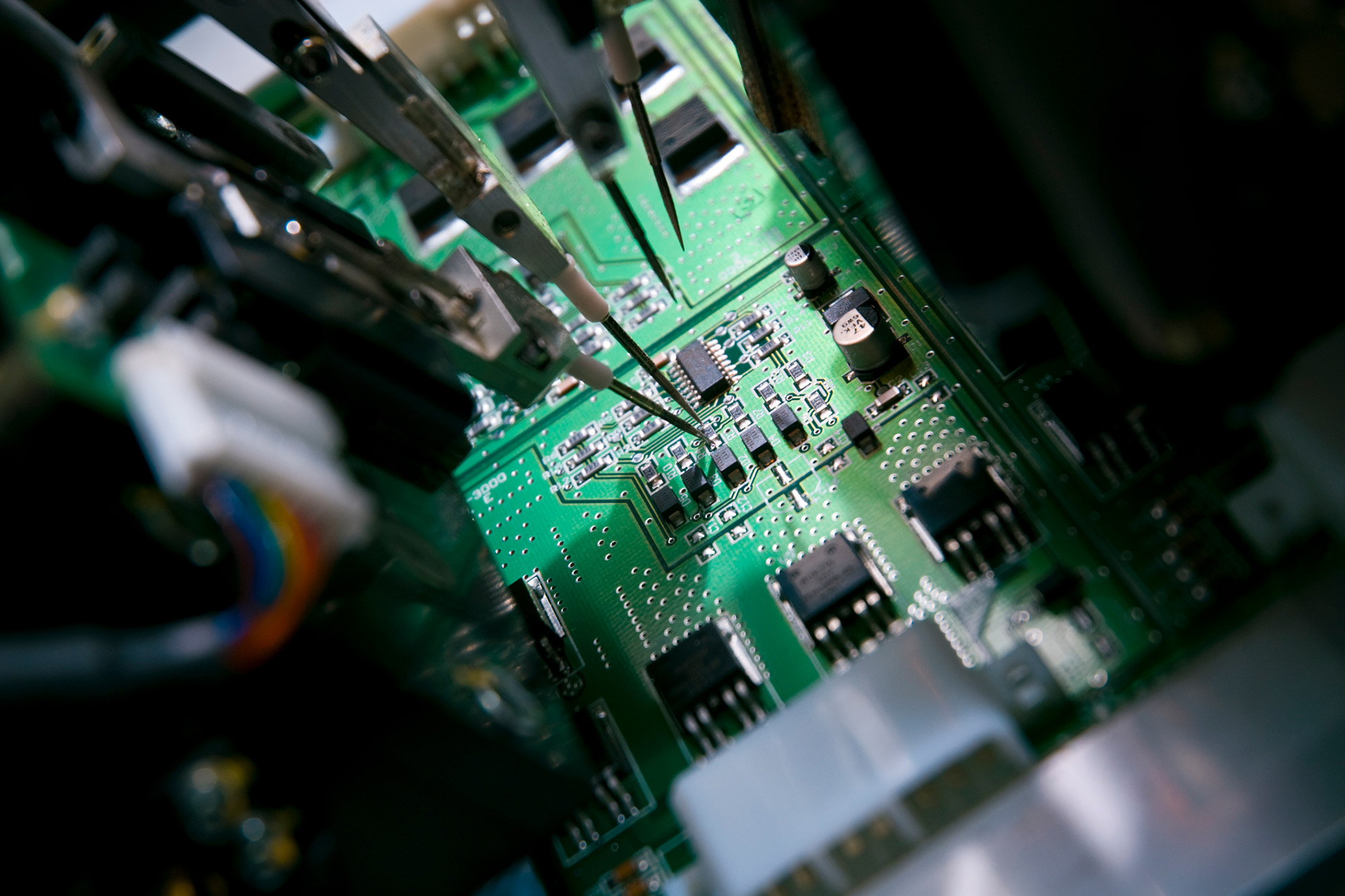
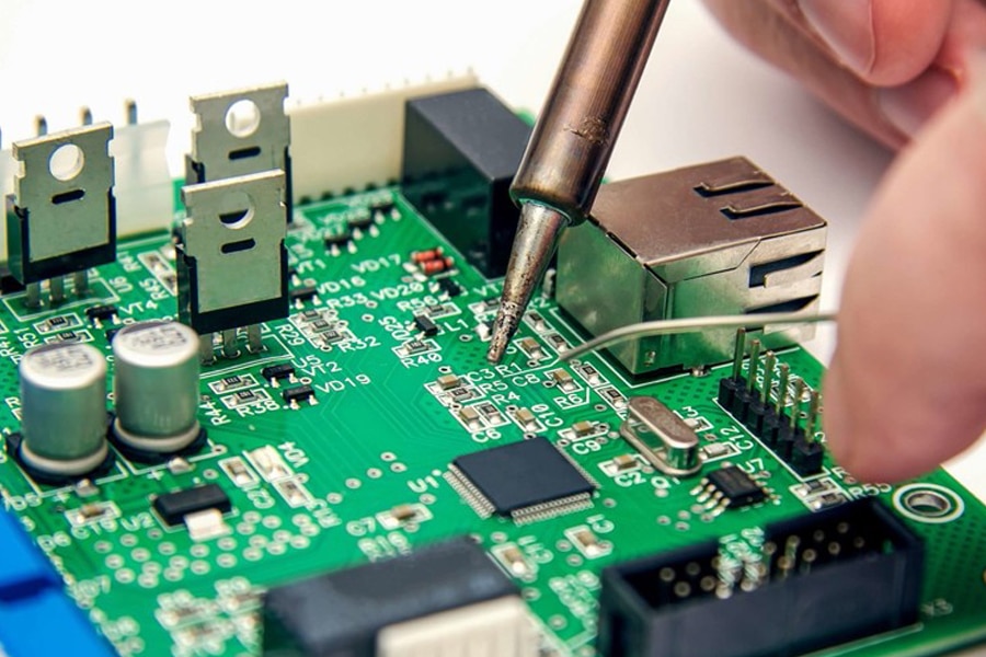
Another challenge is ensuring a precise manufacturing process. Mid-low loss PCBs typically require tight tolerances for trace width, spacing, and layer alignment. Any deviation can result in impedance mismatch and signal attenuation, which can affect performance. Advanced manufacturing techniques such as laser drilling and precision etching are often necessary to achieve the required level of precision.
Future Trends in Mid low loss PCB Technology
As data rates continue to increase, the demand for mid low loss PCB is expected to grow. Emerging technologies such as artificial intelligence, autonomous vehicles, and next-generation wireless communications will require PCBs that can support higher data rates with minimal signal loss. This will drive innovations in materials and manufacturing processes to develop PCBs with lower loss characteristics and higher performance.
One potential trend is the use of hybrid materials that combine the advantages of different dielectric properties to achieve optimal performance. Additionally, advances in manufacturing technologies, such as additive manufacturing and nanotechnology, enable the production of PCBs with unprecedented precision and performance. These developments will help meet the growing demands of high-speed applications and ensure that mid low loss PCBs remain at the forefront of PCB technology.
Choose the Right Mid low loss PCB for Your Application
Mid low loss PCBs are an essential component for applications that require high data rates and signal integrity. Their unique characteristics, such as low dielectric loss and optimized impedance, make them ideal for a wide range of high-speed applications, from telecommunications to data centres. When selecting a mid low loss PCB, it is essential to consider the application’s specific requirements, including data rate, signal integrity, and cost. By choosing the right mid low loss PCBs, you can ensure that your system will operate efficiently and reliably, even at high speeds.