How do you address issues like crosstalk in 6 layer SSD PCB?
In high-performance electronics, the design and fabrication of 6 layer SSD PCB play a vital role in achieving optimal data transfer rates and reliability. As the demand for faster and more efficient storage solutions continues to grow, the complexity of PCB design is also increasing. Among the many challenges facing designers, crosstalk stands out as an essential issue. Crosstalk refers to the unwanted transmission of signals between adjacent traces, which can lead to data corruption and performance degradation. Let’s deeply dive into crosstalk in 6 layer SSD PCB and discuss its causes, effects, and practical strategies to minimize its impact.
Understanding Crosstalk in 6 Layer SSD PCB
Crosstalk is the unwanted transfer of signals between closely placed conductors, leading to potential data corruption and degradation of signal quality. In a 6 layer SSD PCB context, crosstalk can arise from several sources, including capacitive and inductive coupling between adjacent signal traces. As data rates increase and signal frequencies soar, the likelihood of crosstalk becomes a critical concern. This section will delve into the fundamental principles of crosstalk, examining its causes and effects specifically within the realm of SSD PCBs.
To understand the impact of crosstalk, it’s essential to recognize how closely routed traces can interact. Signals travelling through these traces generate electromagnetic fields that can influence adjacent lines. The result is often an unintended signal alteration, leading to data transmission errors. Crosstalk becomes increasingly problematic in high-density designs, where space constraints force traces closer together.

Importance of Proper Layer Stackup Configuration
The stack-up configuration of a 6 layer SSD PCB is critical in minimizing crosstalk and improving overall performance. By carefully planning the arrangement of layers, designers can significantly reduce electromagnetic interference (EMI) and enhance signal integrity. This section will explore the principles of effective layer stack-up and how to arrange the layers to minimize crosstalk, focusing on the strategic placement of signal, power, and ground layers.
Dedicated ground and power planes should be positioned adjacent to signal layers in an ideal stack-up. This proximity creates a stable reference for the signals, helping to isolate them from one another. Differential signalling can also be employed, where pairs of traces carry equal and opposite signals, thus cancelling potential interference. The optimal layer arrangement reduces crosstalk and contributes to improved thermal management and mechanical stability.
Guaranteeing Signal Integrity Using Controlled Impedance Techniques
Controlled impedance is a key factor in high-speed PCB designs, particularly for 6 layer SSD PCBs. Impedance mismatches can lead to signal reflections, which exacerbate crosstalk issues. This section will provide an in-depth look at controlled impedance and explain its significance in minimizing crosstalk and ensuring signal integrity.
Several factors must be considered to maintain controlled impedance, including trace width, spacing, and the dielectric material used in the PCB. By adhering to specific design guidelines, designers can create a consistent impedance profile throughout the board. This practice not only mitigates crosstalk but also enhances overall signal quality. Techniques such as using precise trace widths and maintaining consistent spacing between traces will be discussed, along with the role of simulation tools in validating impedance profiles before manufacturing.

Trace Routing Strategies for Reducing Crosstalk
Effective trace routing is essential for reducing crosstalk in 6 layer SSD PCBs. This section will highlight best practices for routing traces to minimize the potential for signal interference. Strategies such as increasing trace spacing, shortening trace lengths, and maintaining uniform trace widths will be emphasized.
By increasing the distance between high-speed signal traces, designers can significantly reduce capacitive coupling, a primary cause of crosstalk. Shorter traces minimize the area where interference can occur, leading to cleaner signals. Additionally, avoiding unnecessary vias is crucial, as vias can introduce unwanted inductance and further complicate signal integrity. Practical examples and guidelines for effective trace routing will be provided to assist designers in achieving optimal layouts.
The Role of Via Design in Managing Crosstalk
Vias are integral to multilayer PCB design, allowing connections between different layers. However, poorly designed vias can contribute to crosstalk issues. This section will discuss optimizing via design to effectively manage crosstalk in 6 layer SSD PCBs.
To mitigate the impact of vias on signal integrity, designers should consider using blind or buried vias, which minimize exposure and reduce the potential for crosstalk. Additionally, keeping via stub lengths short is essential, as more extended stubs can introduce inductance and compromise signal quality. The strategic placement of vias, along with careful consideration of their type and design, can significantly enhance the PCB’s performance.

Simulating and Testing for Crosstalk in 6 Layer SSD PCB
Simulation and testing are crucial in identifying and addressing crosstalk issues during the design phase of 6-layer SSD PCBs. This section will explore various simulation and testing techniques that engineers can employ to analyze crosstalk effectively.
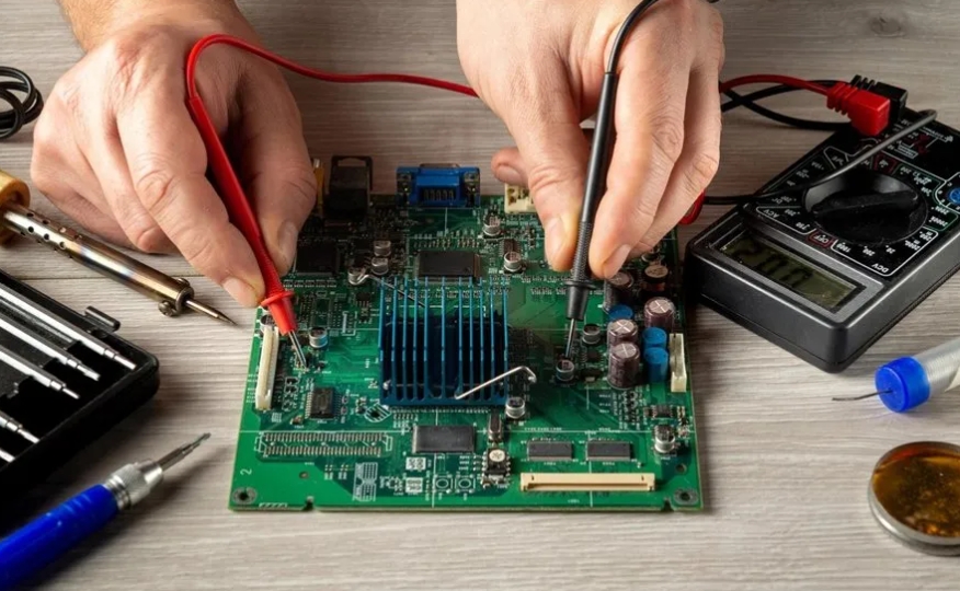
Utilizing advanced simulation software for signal integrity analysis allows designers to visualize potential crosstalk issues before fabricating the PCB. By simulating different routing scenarios and layer configurations, designers can evaluate the impact of their choices on signal integrity. Engineers can also employ real-world testing methods, such as Time Domain Reflectometry (TDR), to assess the effectiveness of the design in minimizing crosstalk. This section will highlight best practices for both simulation and validation to ensure that designs meet performance criteria.
Enhancing Performance in 6 Layer SSD PCB
Effectively addressing crosstalk in 6 layer SSD PCBs is vital for maintaining high performance and reliability in modern electronic devices. By understanding the principles of crosstalk, implementing proper layer stack-ups, utilizing controlled impedance techniques, optimizing trace routing, managing vias, and employing simulation tools, designers can significantly mitigate crosstalk issues.

