
How does an SSD PCB contribute to overall SSD performance?
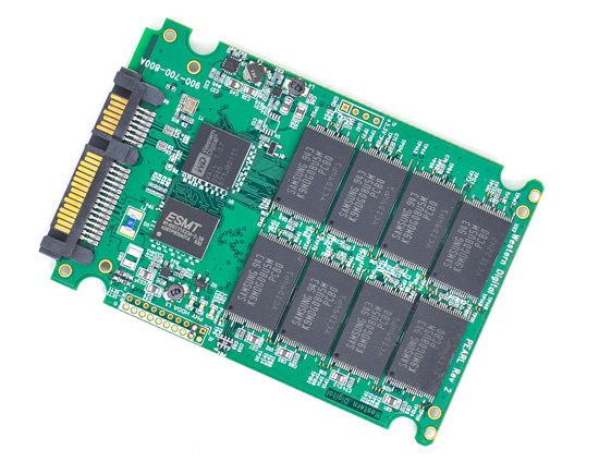
At the heart of every SSD is a complex PCB that is the foundation for all components. More than just a passive structure, the SSD PCB plays a vital role in the performance, durability, and functionality of the SSD. From signal integrity to power management, the SSD PCB’s design and quality directly impact the SSD’s performance. In this article, we will explore the various ways the SSD PCB affects overall SSD performance, giving users and consumers from different industries a detailed understanding of its importance.
Signal Integrity and Its Impact on SSD Performance
One of the most critical aspects of an SSD PCB is its ability to maintain signal integrity. Signal integrity refers to the quality and consistency of electrical signals transmitted through PCB traces connecting the various components of the SSD. The design of the SSD PCB traces plays a vital role in signal integrity. If the traces are too long, short, or improperly routed, it can cause signal attenuation, crosstalk, or electromagnetic interference (EMI). We usually carefully design and lay out the traces to ensure optimal signal integrity, considering impedance matching, trace width, and spacing factors. High-quality PCBs use advanced techniques such as differential signaling and controlled impedance to minimize signal loss and interference.
Power Management and Its Impact on SSD Efficiency
Another critical aspect of SSD PCB that affects SSD performance is power management. The SSD PCB is responsible for distributing power to the various components of the SSD, including NAND flash memory, controller, and DRAM cache, to maximize efficiency and minimize energy loss.
Efficient power distribution is critical to maintaining the performance of the SSD, especially in high-demand environments where the drive may be subject to heavy workloads. Our designers use techniques such as power plane segmentation and decoupling capacitors for optimal power management. Power plane segmentation involves creating separate power planes for different voltage levels or components to reduce noise and increase power delivery efficiency. Decoupling capacitors near key components helps stabilize voltage levels and filter out noise, ensuring that components receive clean and stable power. Power management also affects the reliability and durability of the SSD. Excessive power consumption or poor power distribution can cause increased wear on the NAND flash memory and other components, shortening the drive’s life.
The Role of SSD PCB in Data Integrity and Reliability
One of the key ways that SSD PCBs contribute to data integrity is through error detection and correction mechanisms. Modern SSDs use advanced error correction codes (ECC) to detect and correct errors that may occur during data storage or transmission. The layout of the SSD PCB also plays a role in minimizing the risk of data corruption. By strategically placing components such as the controller, NAND flash memory, and DRAM cache, the PCB can reduce the likelihood of signal degradation or crosstalk, both of which can cause data errors. In addition, our entire design can handle high-speed data transfer without introducing latency or signal distortion, which is critical to maintaining data integrity in high-performance SSDs.
.png)
SSD PCB Design and Its Impact on Speed and Performance
The design of an SSD PCB is a critical factor affecting the speed and overall performance of an SSD. The PCB is the backbone of the drive, connecting all components and enabling the fast and efficient data transfer necessary for a high-performance storage solution. One of the most important aspects of the entire design is the layout of the data path, and the traces on the PCB are carefully designed to minimize resistance and capacitance, both of which slow down data transfer. High-speed SSDs, especially those using the NVMe interface, require PCBs that can handle very fast data rates without introducing latency or signal degradation.
.jpg)
In addition to trace layout, the placement of components on the SSD PCB is also critical to performance. Key components such as the controller, NAND flash memory, and DRAM cache are carefully designed to minimize the distance signals travel. This reduces the possibility of latency and ensures that the SSD can operate at maximum speed.
Customized for Specific Applications
The PCB must be tailored to whether the SSD is used in consumer electronics, enterprise storage, industrial systems, or specialized equipment.
One of the most common areas of customization is the form factor of the SSD PCB. Different applications require different form factors, from compact M.2 and U.2 drives used in laptops and tablets to larger 2.5-inch and 3.5-inch drives used in servers and desktops. The PCB must be designed to fit the specific dimensions of the selected form factor while still accommodating all the necessary components. Another area of customization is the optimization of the power management system. For portable and battery-powered devices, power efficiency is a top priority. You can customize the SSD PCB to minimize power consumption using low-power components and an optimized power delivery network. This extends battery life and reduces heat generation, improving the user experience.
Ultimately
The SSD PCB is an essential component that plays a crucial role in determining the overall performance, durability, and reliability of the SSD. From maintaining signal integrity and power management to ensuring data integrity, speed, and customization, their overall design and quality profoundly impact the drive’s effectiveness.