
How does layer stacking affect the performance of a Multi-layer PCB?
Today, multi-layer PCBs have become necessary for applications ranging from consumer electronics to complex industrial machinery. These PCBs offer significant benefits, including compactness, improved performance, and enhanced electrical characteristics. One key aspect that impacts a multi-layer PCB’s performance is its layer stack configuration. In this blog post, we will take a deep dive into how the layer stack-up affects the overall performance of a multi-layer PCB, providing insights for users and consumers considering these advanced circuit boards.
Understanding the Structure and Function of Multi-layer PCB
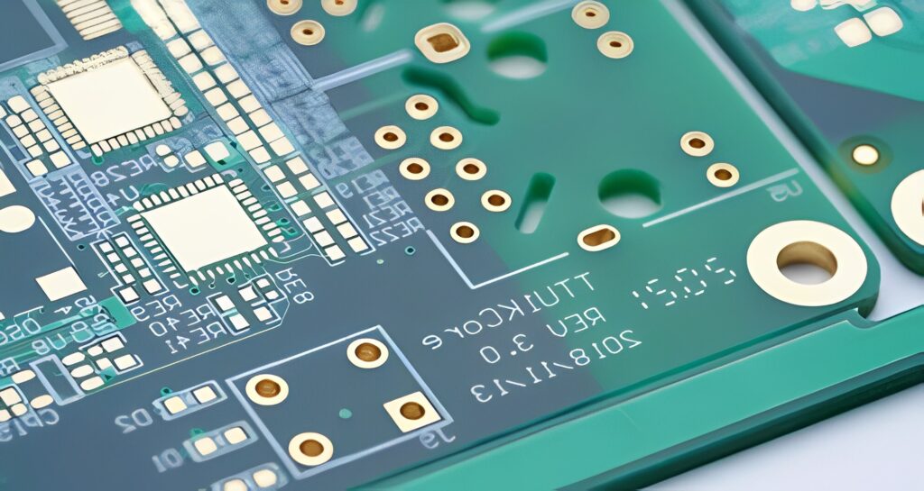
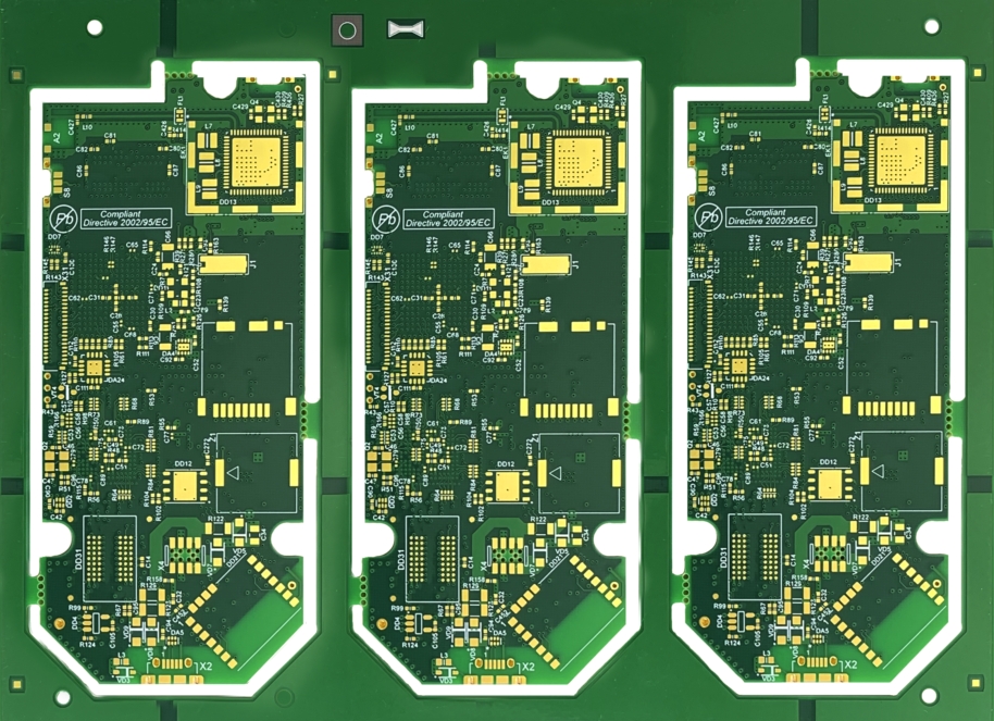
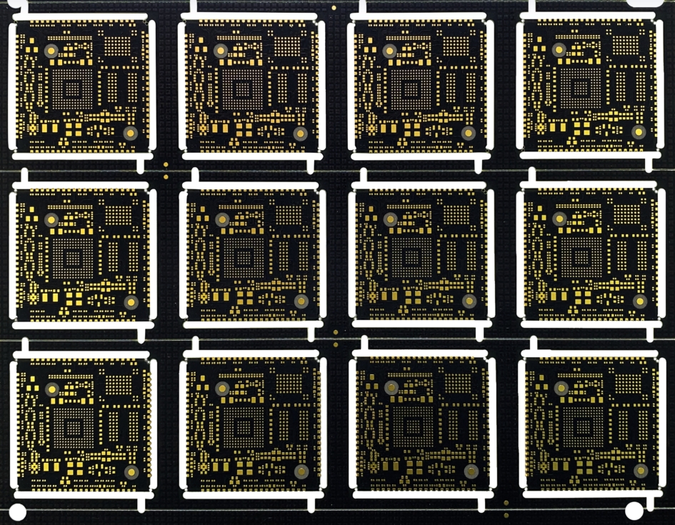
multi-layer PCBs consist of multiple conductive layers separated by insulating layers that enable the interconnection of various electronic components. The most common configurations include two, four, or even up to twelve or more layers, depending on the complexity of the circuit. Each layer serves a different purpose: signal routing, power distribution, or ground plane.
Stacking these layers is more than just a convenience; it plays a critical role in the electrical performance, thermal management, and mechanical stability of the PCB. By understanding the basic structure and function of multi-layer PCBs, users can better understand how the layer stack-up directly affects performance metrics such as signal integrity, impedance control, and electromagnetic interference suppression.
Signal Integrity in Layer Stackup
One of the most critical factors in multi-layer PCB performance is signal integrity, which refers to the quality of electrical signals as they travel through a circuit. Layer stackup directly impacts signal integrity by determining the signal’s routing paths, impedance, and crosstalk susceptibility.
In a well-designed multi-layer PCB, signal layers are typically placed between ground or power planes to shield against external noise and reduce crosstalk. The arrangement of these layers can significantly affect how signals are transmitted, and an incorrect stackup can result in signal degradation. By understanding the relationship between layer stackup and signal integrity, users can make informed decisions when designing or selecting a multi-layer PCB for their application.
Thermal Management in Layer Stackup
Thermal management is another critical aspect of how layer stackup affects multi-layer PCBs. As electronic devices become more compact and powerful, the heat generated by components can present significant challenges. Effective thermal management ensures the PCB can dissipate heat effectively to maintain optimal operating temperatures.
Layer stackup can impact thermal performance by determining the paths available for heat dissipation. For example, incorporating thermal vias and dedicated thermal layers can enhance heat transfer away from heat-generating components. Using materials with high thermal conductivity in specific layers can also improve heat dissipation. Understanding these dynamics is critical for users aiming to optimize the thermal performance of their multi-layer PCBs.
Electromagnetic Interference Suppression in Multi-layer PCB
Electromagnetic interference (EMI) is a significant concern in modern electronic design because it can adversely affect the functionality and reliability of a device. Layer stack-up is vital in mitigating EMI by strategically placing ground and power planes within a PCB.
By placing ground planes near signal layers, designers can create a controlled environment that minimizes the effects of EMI on sensitive signals. Layer arrangement also affects the overall electromagnetic compatibility of the PCB. Users should consider how layer stackup affects EMI suppression to ensure the reliability of their electronic products, especially in interference-sensitive applications.
Impact of layer stack up on mechanical stability
The mechanical stability of a multi-layer PCB is critical to ensure its durability and lifespan, especially in applications subject to physical stresses such as vibration or thermal cycling. Layer stack-up affects the mechanical properties of the PCB, including its stiffness, flexural strength, and warpage resistance.
When the layer stack up is correct, the mechanical integrity of the PCB is enhanced, allowing it to withstand external forces without compromising its performance. Conversely, improper stacking or insufficient support can lead to issues such as delamination or warping, which can ultimately affect the reliability of the circuit. Understanding the interaction between layer stacking and mechanical stability can help users select the correct configuration for their specific application.

Factors Affecting Layer Stacking Costs
While the technical advantages of multi-layer PCBs are clear, users must also consider the cost implications associated with layer stacking. Generally, the more layers a PCB has, the higher the manufacturing complexity and cost. However, the benefits of performance, functionality, and space savings often justify these additional expenses.
Users should evaluate their needs and applications to determine the best layer configuration that balances performance requirements and budget constraints. Working with an experienced PCB manufacturer can also provide insights into cost-effective solutions without sacrificing quality. Understanding the economic aspects of layer stacking can lead to more informed purchasing decisions.
Future Trends and Developments in Layer Stacking
The design and manufacturing of multi-layer PCBs is evolving rapidly as technology advances. Emerging trends such as miniaturization, increased component integration, and the need for higher performance metrics are influencing how layer stacking is handled.
Innovative materials and manufacturing techniques, including additive manufacturing and advanced dielectric materials, make it possible to create thinner, lighter, and more efficient multi-layer PCBs. As these trends continue to impact the PCB design landscape, users must stay current on the latest advances and best practices in layer stacking to fully realize their multi-layer PCBs’ potential.
Impact of Layer Stackup on Multi-layer PCB Performance
Layer stackup is a fundamental aspect that significantly affects the performance of multi-layer PCBs. From enhancing signal integrity and thermal management to mitigating EMI and ensuring mechanical stability, the arrangement of layers plays a vital role in determining the overall efficiency of these boards.