
How does ultra low loss PCB affect signal-to-noise ratio (SNR)?
The need for ultra low loss PCB is increasing in high-frequency and high-speed applications. These specialized PCBs minimize signal loss, ensuring the signal maintains integrity as it travels across the board. One of the key metrics that impact ultra-low loss PCBs is the signal-to-noise ratio (SNR), which measures signal clarity in the presence of noise. This blog post will explore the relationship between ultra-low loss PCBs and SNR.
The Role of ultra low loss PCB Materials in Improving SNR
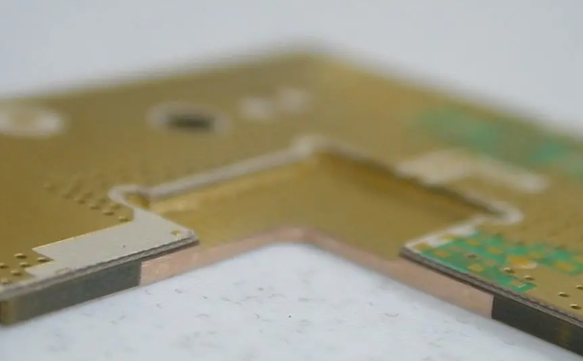
In ultra low loss PCB, the right substrate material is essential to ensure minimal signal attenuation and excellent SNR. The material’s dielectric constant (Dk) and dissipation factor (Df) are central to this selection process. The dielectric constant determines how much electrical energy a material can store, while the dissipation factor indicates how much energy is lost as heat. We use materials with low Dk and Df values for ultra low loss PCBs. These properties ensure the signal propagates with minimal distortion and energy loss, maintaining signal integrity. One of the most popular materials in this category is polytetrafluoroethylene (PTFE), commonly known as Teflon. PTFE-based substrates have very low dielectric constants and dissipation factors, making them ideal for high-frequency applications.
Design Strategies for Ultra Low Loss PCBs to Optimize Signal-to-Noise Ratio
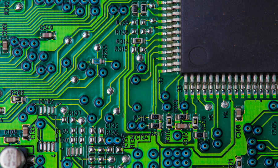
While material selection lays the foundation for ultra-low loss PCBs, certain design strategies must be adopted to improve the SNR. One of the main design considerations is to implement controlled impedance traces. Designing traces with specific impedance values can minimize signal reflections and mismatches. This is especially important in high-frequency applications, where impedance discontinuities can cause severe signal attenuation. Another key strategy is to utilize differential signalling. Differential pairs can effectively cancel common-mode noise. This technique improves SNR and the system’s immunity to electromagnetic interference (EMI). In addition, layer stackup, signal trace routing, and component placement play a key role. The placement of key components should minimize trace lengths and reduce potential signal delays and losses.
Signal Attenuation and Its Effect on SNR
Signal attenuation is the reduction in signal strength as it propagates through a PCB transmission line. In ultra low loss PCBs, attenuation is caused by various factors, including the resistance of the conductor, dielectric losses in the material, and the transmitted signal’s frequency.
Ultra low loss PCBs minimize signal attenuation by using high-quality materials with low resistivity and optimizing transmission line design. For example, wider or thicker copper lines can reduce resistance, reducing signal attenuation. Similarly, using low-loss dielectric materials helps minimize the energy lost as heat in the dielectric, maintaining signal strength and a higher SNR.
Another important design consideration is the impedance matching of the transmission line. Proper impedance matching ensures that the system transfers maximum signal energy from the source to the load while minimizing reflections, which can cause signal attenuation and reduce SNR. By focusing on reducing signal attenuation, ultra-low loss PCBs play a key role in maintaining SNR, especially in high-frequency and high-speed applications.
The Effect of Crosstalk on SNR and How to Mitigate It
Crosstalk is another important factor affecting a PCB’s signal-to-noise ratio (SNR). Crosstalk occurs when a signal travelling on one trace creates an unwanted signal on an adjacent trace, causing interference and potential data corruption. Ultra low loss PCBs have features that help mitigate crosstalk, thereby maintaining SNR. One of the main ways to reduce crosstalk is to carefully manage the spacing between traces.
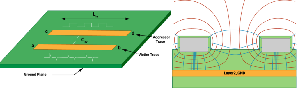
To combat this, ultra low loss PCBs often employ ground planes and shielding techniques. A copper layer between signal layers provides a return path for current and shields the signal as a ground plane. By strategically placing ground planes and using them effectively, designers can significantly reduce crosstalk and maintain a higher SNR.
Applications that enhance signal-to-noise ratio
One application that stands out is high-frequency communication systems. As 5G networks and beyond become more prevalent, the need for PCBs that can handle gigahertz frequencies without significant signal loss is critical. Ultra-low loss PCBs ensure the system transmits data with minimal attenuation, maintaining the high SNR necessary for clear and reliable communications. Radar systems, satellite communications, and avionics require PCBs that can perform flawlessly under harsh conditions. Ultra low loss PCBs provide excellent signal integrity and resilience, ensuring the system transmits and receives critical data without impairment.
Maintaining a high SNR is critical for accurate diagnosis in medical devices, especially imaging devices such as MRI and CT scanners. Ultra low loss PCBs ensure that electronic signals are processed with minimal noise, improving the clarity and precision of imaging and improving patient outcomes.
Play a key role in optimizing signal-to-noise ratio.
From understanding the fundamentals of how material properties affect signal propagation to exploring advanced design strategies to mitigate potential signal integrity challenges, achieving high SNR is a multifaceted endeavor. Manufacturing precision further ensures that the theoretical advantages of design and material selection are realized in the physical product, thereby maintaining signal integrity as the signal traverses a complex electronic environment. The applications of ultra-low loss PCBs are very wide, from cutting-edge communication systems to life-saving medical devices, highlighting their versatility and indispensability.