
How to prevent crosstalk in mid low loss pcb?
Crosstalk is a significant problem in PCBs, shallow- and medium-loss ones. Crosstalk refers to the unwanted coupling of signals between adjacent traces or layers, which can lead to signal degradation, data errors, and overall performance issues. This guide will introduce various strategies and techniques to mitigate crosstalk in mid low loss PCB to achieve excellent PCB performance.
Crosstalk in mid low loss PCB
Crosstalk occurs when a signal traveling on one trace or conductor has an undesirable effect on an adjacent trace and is a significant concern in high-speed digital and RF applications. In mid low loss pcbs, crosstalk can offset the benefits of low-loss materials and advanced design to minimize signal degradation and dielectric losses. Capacitive crosstalk originates from electric fields between adjacent traces, while inductive crosstalk originates from magnetic field coupling. Trace spacing, signal frequency, and PCB layout affect both crosstalk types. Designers need to use careful design and layout practices to address these factors and reduce the impact of crosstalk on mid low loss PCBs.

Optimal Trace Spacing in mid low loss PCB
Optimal trace spacing is one of the most effective ways to prevent crosstalk in mid low loss PCBs. Increasing the distance between signal traces reduces electric and magnetic field interactions, thereby minimizing capacitive and inductive crosstalk. Generally, we adopt a trace spacing of at least three times the trace width. However, a larger spacing may be required for high-speed and high-frequency applications. In addition, we also implement uniform trace width and spacing on mid low loss PCBs to maintain consistent impedance and reduce signal reflections. We properly manage the spacing between signal traces and other conductive elements to maintain signal integrity and prevent crosstalk in mid-low loss PCBs.

Use Ground Planes
Ground planes prevent crosstalk by providing a return path for signals and reducing the loop area for current flow. In mid low loss pcbs, we use a continuous and solid ground plane under the signal layer to effectively shield the traces, thereby reducing capacitive and inductive coupling. The ground plane also helps maintain a consistent reference voltage, critical for high-speed signal integrity. A dedicated ground plane between signal layers in mid low loss PCBs can further isolate signals and reduce crosstalk. To ensure proper grounding practices, minimizing via transitions and avoiding split ground planes are essential to maximize the effectiveness of the ground plane in preventing crosstalk.
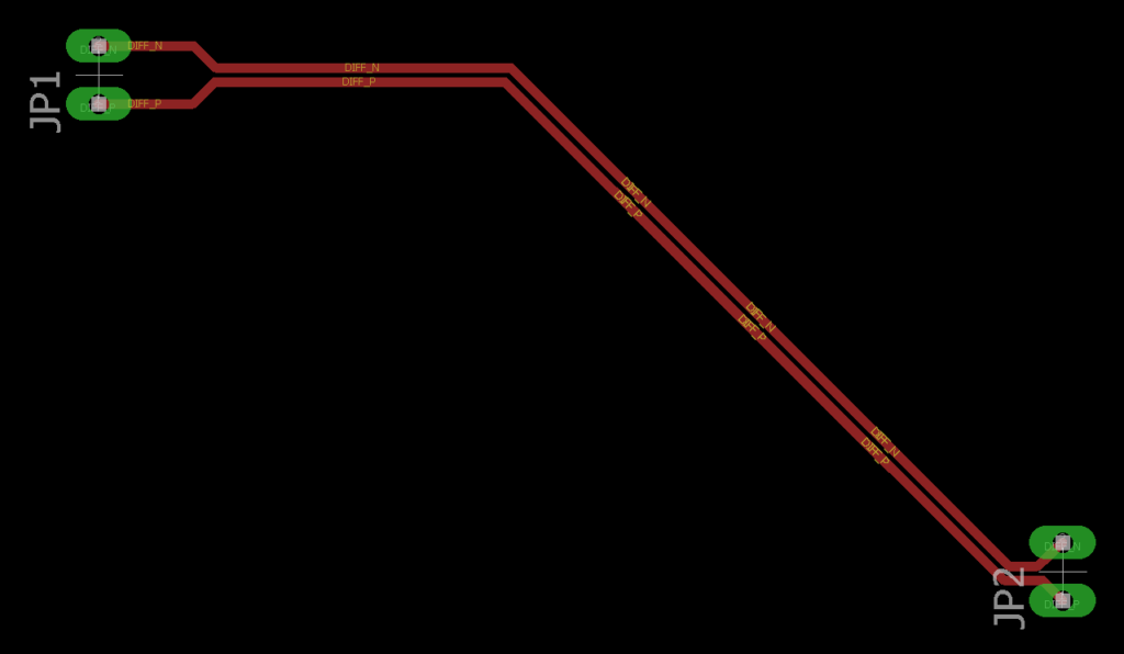
Differential Pair Routing
Differential pair routing is a technique for mitigating crosstalk by routing two complementary signal lines nearby, which exploits the principle of differential signaling, where the signals are equal in amplitude but opposite in polarity. Routing differential pairs with consistent spacing and symmetry effectively cancel crosstalk induced in one line with the opposite signal in the other line. For mid low loss PCB, differential pair routing helps reduce crosstalk and enhances noise immunity and signal integrity.
Implementing Guard Traces
Guard traces, also known as guard strips, are additional traces placed between signal lines to shield against crosstalk. These traces are typically connected to a low-impedance reference point and act as a barrier to electric and magnetic fields. In mid low loss pcbs, strategically placing guard traces between critical signal lines can significantly reduce capacitive and inductive coupling. Ensuring proper grounding and maintaining consistent spacing with the signal line is key to the performance of a guard line, as its effectiveness depends on its location and connection. In addition, using multiple guard lines or stitching vias to connect the guard line to the ground plane can enhance its shielding capabilities.
Ensure Optimal Performance
Preventing crosstalk is critical to designing high-performance, mid low loss PCB. To address this issue, we implemented effective design strategies such as optimal trace spacing, ground planes, differential pair routing, guard traces, and other techniques to address the crosstalk issue.