
Key Features of High Quality 2 layer OSP PCB
Among various types of PCBs, 2 layer OSP PCB is popular for their unique combination of simplicity, reliability, and cost-effectiveness. OSP is a widely used PCB surface finish that helps protect copper pads during soldering. This blog post will delve into the main features of high-quality 2-layer OSP PCBs so that more users who use them can understand them better.
Structure and Composition of 2 layer OSP PCB
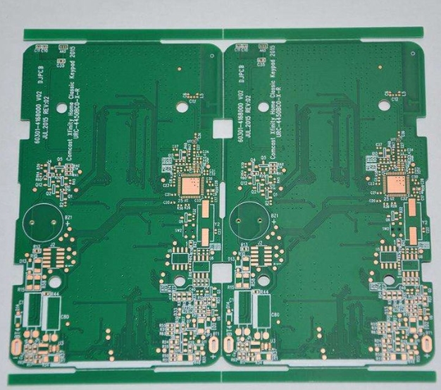
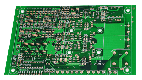
High-quality 2 layer OSP PCBs are characterized by a simple and efficient structure. It consists of two copper conductive layers separated by an insulating layer in the middle. Compared with single-layer PCBs, this structure allows for more complex circuit designs while still maintaining a certain degree of simplicity. In terms of substrate materials, they use FR-4, a glass-reinforced epoxy laminate that is the most common choice due to its excellent mechanical strength, electrical insulation properties, and heat resistance. Manufacturers of high-quality 2-layer OSP PCBs will use a sufficient thickness of copper, and they will use thicker copper layers for higher current carrying capacity and lower resistance.
OSP coating is a key feature of 2 layer OSP PCB. A thin organic film coats the copper surface to prevent oxidation before soldering. This coating is very effective in maintaining solderability, ensuring that the copper pads remain pristine and oxidation-free.
Advantages of Using 2-layer OSP PCBs
2-layer OSP PCBs offer various advantages stemming from their design, materials, and OSP surface treatment.
- Cost-effectiveness:
One of the most significant advantages of 2-layer OSP PCBs is cost-effectiveness. The manufacturing process of these PCBs is relatively simple, requiring less materials and machinery than multi-layer PCBs. The OSP coating process is also cheaper than other surface treatment processes such as ENIG or HASL. - Enhanced Solderability
The primary purpose of OSP coating is to improve solderability. By preventing copper oxidation, OSP ensures that solder joints are solid and reliable. This is especially important for fine-pitch components and high-density PCBs, where solderability issues can lead to defects and failures. - Environmentally friendly
OSP is an environmentally friendly surface treatment process. It does not contain heavy metals such as lead, making it a safer choice for manufacturers and end users. In addition, the OSP coating process produces less waste than other surface treatment processes. - Simple and Reliable
2-layer designs strike a balance between complexity and simplicity. While more complex than single-layer PCBs, they are easier to design, manufacture, and troubleshoot than multi-layer boards. This simplicity means higher reliability and lower production costs.
Main Applications
High-quality 2-layer OSP PCBs are widely used in various industries due to their versatility and reliability. In consumer electronics, 2-layer OSP PCBs are widely used in smartphones, tablets, and wearable devices. The demand for compact, reliable, cost-effective PCBs makes 2-layer OSP PCBs an ideal choice.

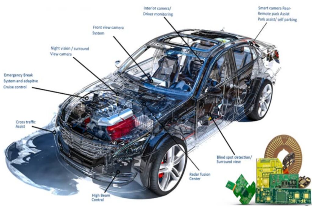
In industrial applications, rugged and reliable PCBs are often required to withstand harsh environments and demanding usage conditions. They suit industrial control systems, motor drives, and automation equipment. The durability of the FR-4 substrate combined with the protective OSP coating ensures that these PCBs can withstand high temperatures and chemical attacks without compromising performance. In the automotive industry, 2-layer OSP PCBs are used in various automotive applications, including engine control units, infotainment systems, and lighting systems.
Quality Control and Testing
To ensure the characteristics of 2 layer OSP PCB, a comprehensive quality control and testing program is required for their quality and reliability. Visual inspection is the first line of defense for quality control. Our technicians check for any visible defects on the PCB, such as misaligned components, incomplete solder joints, or surface defects. Electrical testing is essential to verify the functionality of 2-layer OSP PCBs. This includes continuity testing to ensure that all electrical connections are intact and isolation testing to verify that there are no shorts between traces. Additionally, functional testing involves verifying that they operate as expected in the final application. This may include powering up the PCB, simulating operating conditions, and measuring key performance parameters, among other things.
Future Trends and Innovations
The field of 2-layer OSP PCB manufacturing continues to evolve, with new technologies and innovations emerging to achieve higher performance, reliability, and sustainability. Innovations in OSP formulations are enhancing the protective capabilities of coatings. New OSP solutions offer better thermal stability, longer shelf life, and improved solderability, making them suitable for a wider range of applications. Additionally, the convergence of IoT and smart technology is creating new opportunities for 2-layer OSP PCBs. These PCBs are being used in connected devices and smart systems, where reliable performance and cost-effectiveness are critical, and miniaturization and HDI trends are pushing the limits of 2-layer OSP PCB design.
The Value of High-Quality 2-Layer OSP PCBs
High-quality 2-layer OSP PCBs combine reliability, cost-effectiveness, and versatility, making them ideal for a wide range of applications. From consumer electronics and industrial equipment to medical devices and telecommunications, they feature the performance and durability required to meet the demands of modern technology.