
Layer Stackup Design for Heavy Copper PCB: Maximizing Performance
The Heavy Copper PCB is essential for high-power and high-current applications, but its performance heavily depends on proper layer stack-up design. A well-planned stack-up ensures optimal electrical performance, thermal management, and mechanical stability. This blog dives into the key principles of layer stack-up design for Heavy Copper PCBs, offering practical tips to maximize their performance.
Understanding Layer Stackup Design for Heavy Copper PCB
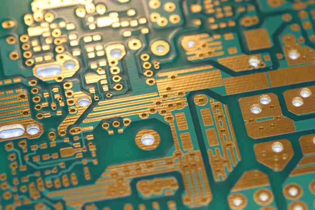
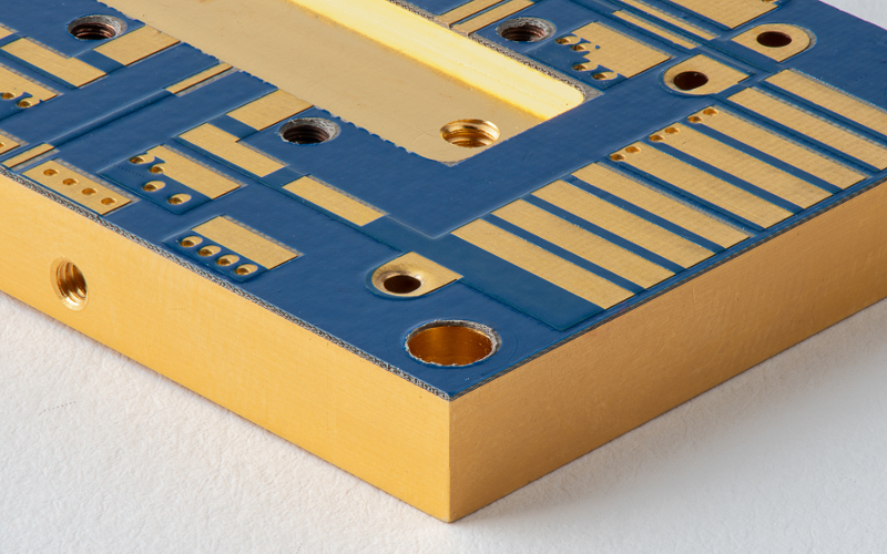
Layer stackup refers to the arrangement of copper layers, dielectric materials, and insulating layers in a PCB. For Heavy Copper PCB, the stack-up design must account for the increased copper thickness, ranging from 3 oz to 20 oz or more. This requires careful planning to balance electrical performance, thermal dissipation, and mechanical strength.
The primary goal of a Heavy Copper PCB stackup is to minimize signal loss, reduce electromagnetic interference (EMI), and manage heat effectively. By optimizing the layer arrangement, you can ensure that the PCB meets the demands of high-power applications while maintaining reliability and durability.
.jpg)
Key Considerations for Stackup Design
Several factors must be considered when designing a stackup for Heavy Copper PCB. First, determine the number of layers based on the complexity of the circuit and the current requirements. More layers allow for better signal integrity and power distribution but increase manufacturing complexity and cost.
Next, consider the copper weight and its distribution across layers. Heavy Copper PCBs often use thicker copper for power and ground planes to handle high currents. Ensure the dielectric materials between layers can support the increased copper thickness without compromising insulation or mechanical stability.
Optimizing Heavy Copper PCB Signal Integrity
Signal integrity is critical in Heavy Copper PCBS, especially for high-frequency applications. Place signal layers adjacent to ground planes to minimize signal loss and crosstalk. This creates a controlled impedance environment, reducing noise and improving signal quality.
Use microstrip or stripline configurations for high-speed signals. Microstrip routing places signals on the outer layers, while stripline routing embeds them between ground planes. Both methods help maintain signal integrity, but stripline offers better EMI shielding for Heavy Copper PCB.
Effective Thermal Management
Due to high current flow, heavy copper PCBs generate significant heat. Effective thermal management is essential to prevent overheating and ensure long-term reliability. To dissipate heat efficiently, incorporate thermal vias and heat sinks into the stack design.
Place power and ground planes close to the surface layers to improve heat dissipation. Use thermally conductive dielectric materials to enhance heat transfer between layers. Proper thermal management extends the PCB’s lifespan and enhances its performance under high-power conditions.
Power Distribution and Current Handling
Heavy Copper PCBs are designed to handle high currents, making power distribution a critical aspect of stack-stack-up design. Use thick copper layers for power and ground planes to reduce resistance and minimize voltage drops. Ensure the paths are wide enough to handle the expected current without overheating.
Incorporate multiple power and ground planes to distribute current evenly across the PCB. This reduces the risk of localized heating and improves overall performance. For multi-layer Heavy Copper PCB, alternate power and ground planes to create a low-impedance power distribution network.
Ensuring Mechanical Stability
The increased copper thickness in Heavy Copper PCBs can affect mechanical stability. To ensure durability, use robust dielectric materials that can withstand the mechanical stress caused by heavy copper layers. Consider the materials’ coefficient of thermal expansion (CTE) to prevent warping or delamination during thermal cycling.
Incorporate stiffeners or additional support layers, especially for large or complex Heavy Copper PCBs if necessary. Proper mechanical design ensures the PCB can withstand harsh operating conditions without compromising performance.
Manufacturing Considerations
Manufacturing Heavy Copper PCB requires specialized processes and equipment. Communicate clearly with your PCB manufacturer to ensure your stackup design is feasible. Provide detailed specifications for copper thickness, dielectric materials, and layer arrangement.
Consider the impact of heavy copper on etching, plating, and lamination processes. Heavy Copper PCB may require additional steps, such as step plating or controlled-depth drilling, to achieve the desired layer stack. Collaborate with your manufacturer to optimize the design for manufacturability.
Maximizing Performance with Heavy Copper PCB Layer Stackup
Layer stack-up design is critical to maximizing the performance of Heavy Copper PCBs. You can create a PCB that meets high-power applications by optimizing signal integrity, thermal management, power distribution, and mechanical stability.
When designed correctly, Heavy Copper PCBs offer unparalleled performance and reliability. Whether working on industrial equipment, renewable energy systems, or automotive electronics, a well-planned stack ensures that your Heavy Copper PCB delivers optimal results. Embrace these design principles to unlock the full potential of Heavy Copper PCBs in your projects.