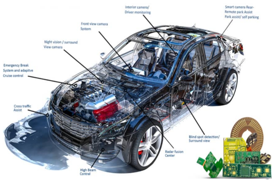
Double side PCB, short for double-sided printed circuit boards, are the workhorses of the electronics industry. They provide a versatile and efficient platform for connecting electronic components in various devices, from your smartphone and computer to your car’s engine control unit. In this introduction, we’ll delve into what double-sided PCBs are, their essential parameters, and the manufacturing process that brings them to life.
Key Parameters of Double-Sided PCBs
Number of Layers: A double-sided PCB consists of two layers of substrate material, separated by a core layer. Copper traces are etched on both sides, allowing for more complex circuits and higher component density.
Size: Double-sided PCBs come in a variety of sizes and shapes and can be tailored to the specific requirements of the device in which they are used. Standard sizes (such as 4×6 inches) are typical, but custom sizes are available for unique applications.
Copper Thickness: The thickness of the copper layer on a double-sided PCB is measured in ounces per square foot (oz/ft²). Standard thicknesses include 1 oz and 2 oz, with thicker copper providing better current carrying capabilities.
Hole Size: Double-sided PCBs have holes for component leads or connectors. The accuracy and size of these holes are critical to ensuring proper component alignment and soldering.
Solder mask and silk screen: Solder mask is a protective layer applied to the PCB to prevent solder bridges and corrosion. A silkscreen layer is used for component markings and indicators.
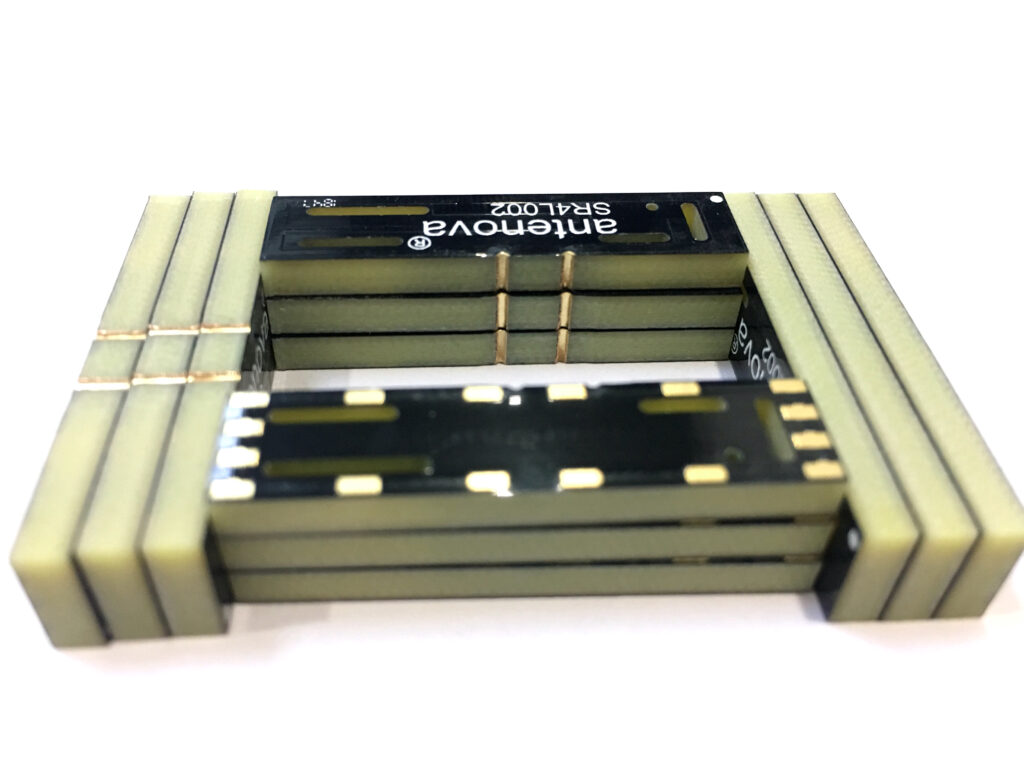
If necessary, you can click to view more of our cases.
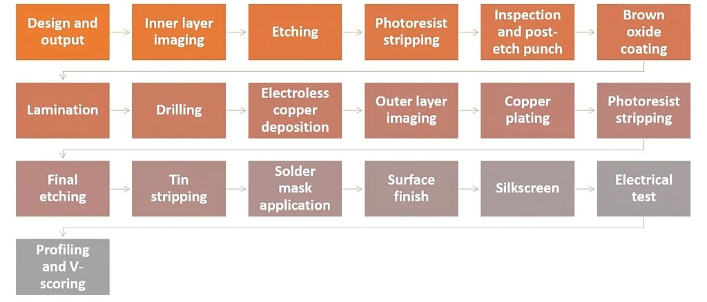
The production of a double-sided PCB involves several key steps:
Substrate preparation: The substrate (usually fiberglass epoxy) is cut to standard or custom sizes. It is then cleaned and prepared for the copper foil lamination process.
Copper Cladding: Copper foil is laminated to both sides of the substrate using heat and adhesive. These foils will become the conductive traces on the PCB.
Circuit Design: Computer-aided design (CAD) software creates the circuit design of a PCB, including trace and component placement.
Etching: Using chemicals to etch away unwanted copper, leaving the desired traces and pad patterns.
Drilling: Drill holes for components and vias, which are small holes used to connect traces on different layers. This step requires precision to ensure members are aligned.
Plating: Plating holes with copper to enhance their conductivity and ensure a strong connection.
Solder Mask and Screen Printing: Multi-layer solder mask and screen printing protect and mark PCBs.
Testing: To ensure functionality and reliability, double-sided PCBs require electrical testing, including continuity checks and insulation resistance testing.
Advantages of Heavy Copper PCB
✔ Increased Circuit Density: Supports more complex circuits than single-layer PCBs.
✔ Compact Design: Ideal for space-constrained applications.
✔ Improved Electrical Performance: Reduced interference and better signal integrity.
✔ Cost-Effective Solution: Balances complexity and affordability.
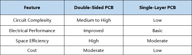
Double-Sided PCB VS. Single-Layer PCB
Why Choose Us
Competitive Pricing
More than a decade of experience in the PCB industry ensures quality components at competitive prices.
Fast and reliable delivery
Partnership with multiple global logistics providers ensures timely and reliable shipping.
Quality Assurance
A dedicated quality control team conducts manual visual inspections to ensure all products meet strict quality standards.
We have many international certifications
We also hold several international quality certifications:
At the same time, we are always committed to environmental protection. We have an environmental management system certification to ensure that our manufacturing process is environmentally friendly and sustainable.
Frequently Asked Questions(FAQ)
What materials are used for Double-Sided PCBs?
We offer FR4, high-TG, CEM-3, and flexible substrates based on application needs.
What is the standard copper thickness for Double-Sided PCBs?
Our standard copper thickness ranges from 1oz to 4oz, with customization options available.
How can I request a custom Double-Sided PCB?
Contact us with your design files, and we will provide a quote within 24 hours.