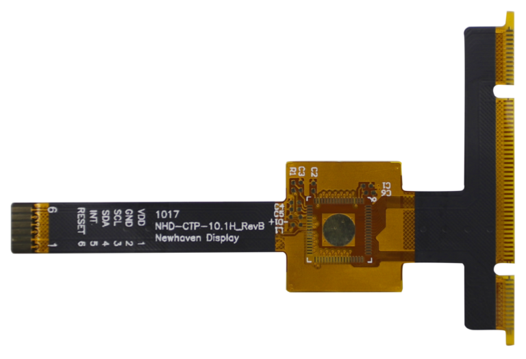
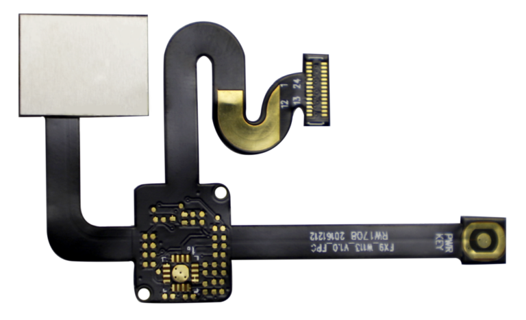
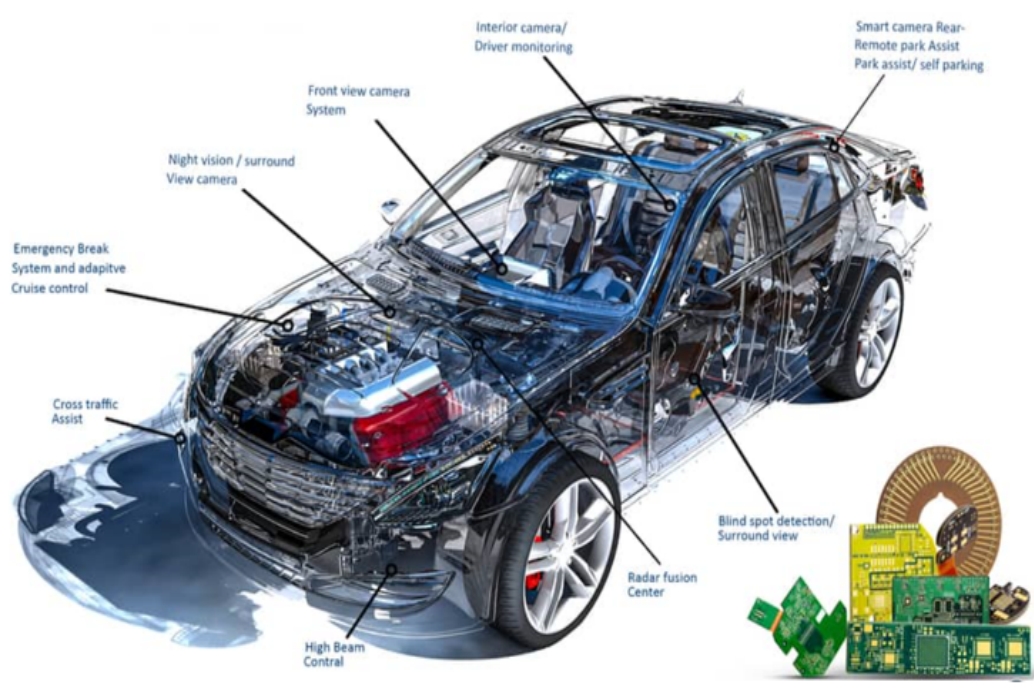
FPC PCB is a flexible circuit board usually constructed of flexible insulating substrate and conductive copper foil, especially when flexibility is required and space is limited. They are widely used in mobile devices, medical devices, automotive electronics and many other fields.
FPC PCB parameters:
1. Substrate type: FPC PCBs usually uses flexible polyester film, polyimide (PI) or polyimide copper-clad foil as the substrate. These substrates offer high temperature resistance, chemical resistance and mechanical strength.
2. Conductive layer: Copper foil is usually used as the conductive layer. The thickness of the copper foil can be customized according to needs, usually between 1oz (ounces per square inch) and 3oz.
3. Thickness: FPC PCB is usually very thin, and its thickness is usually between 0.05 mm (50 microns) and 0.5 mm (500 microns).
4. Circuit line width and spacing: These parameters determine the conductive properties of the circuit. Line width and spacing selection depends on current loading, voltage requirements and the needs of the specific application.
5. Bending radius: The bending radius of an FPC PCB refers to the minimum radius at which the manufacturer can safely bend the circuit board. This parameter is very important as it affects the durability of the board.
6. Pad and Connector Type: These parameters depend on how the FPC PCB is connected to other electronic components or devices. Pad and connector types can be customized to suit specific application needs.
7. Operating temperature range: The operating temperature range of FPC PCB depends on the material selection of the base material and conductive layer. Some FPC PCBs can operate in extreme temperature conditions.
If necessary, you can click to view more of our cases.
Manufacturing process:
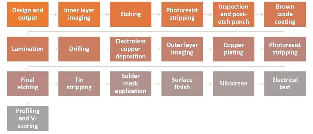
The manufacturing of FPC PCB usually includes the following steps:
Printing: The conductive lines of FPC PCB are generally manufactured on the substrate through printing technology or photolithography process.
Copper foil attachment: For double-sided FPC PCB, the copper foil is attached to the substrate through an adhesive or lamination process to form a double-sided conductive layer.
Etching: Using a chemical etching process to remove unwanted portions of copper foil to create a circuit pattern.
Electroplating: Increasing the thickness of copper foil through the electroplating process to improve the electrical conductivity of a circuit.
Cutting and Forming: Technicians often cut and form FPC PCBs to specific shapes and sizes.
Testing and Quality Control: Technicians perform testing and quality control at all stages of the manufacturing process to ensure that boards meet specifications.
Advantages of FPC PCB PCB
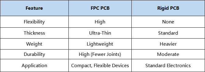
✔ Lightweight & Thin: Reduces overall device weight and thickness.
✔ Highly Flexible: Adapts to complex and dynamic shapes.
✔ Enhanced Reliability: Fewer solder joints reduce failure points.
✔ Excellent Heat Dissipation: Polyimide materials withstand high temperatures.
✔ Improved Signal Integrity: Shorter paths reduce signal loss and interference.
FPC PCB VS. Rigid PCB
Why choose us:
Competitive Pricing: With more than a decade of experience in the PCB industry, we have established a reliable supply chain that ensures quality components at competitive prices. For complex projects requiring unique materials or advanced technical specifications, our strong manufacturing capabilities enable us to provide cost-effective solutions while maintaining high quality.
Fast and reliable delivery: We ensure fast production and delivery. Our partnership with multiple global logistics providers guarantees timely and reliable transportation, supported by our digital factory management and 90% automation for greater efficiency.
Quality Assurance: Our rigorous quality inspection begins with incoming material checks. We use AOI to detect defects and X-rays to identify internal issues. Electrical performance testing is performed with advanced automatic test machines and flying probe testers. Before shipment, our dedicated QC team conducts a thorough manual visual inspection to ensure all products meet strict quality standards.
We have many international certifications:
We also hold several international quality certifications:
●IATF 16949:2016
●ISO 9001:2015
●ISO 45001:2018
●UL
At the same time, we are always committed to environmental protection. We have an environmental management system certification to ensure that our manufacturing process is environmentally friendly and sustainable.





Frequently Asked Questions(FAQ)
- What form factors do you support?
We manufacture SSD PCBs for M.2, U.2, 2.5-inch, and custom designs.
- Can I request a custom SSD PCB layout?
Yes! Our team provides tailored PCB designs based on your SSD specifications.
- How do I get a quote?
Contact us with your design requirements, and we’ll provide a quote within 24 hours.

