Heavy Copper or thick copper PCBs are specialized circuit boards designed for high-current applications. These PCBs feature copper layers thicker than the standard, typically ranging from 3oz to 20oz, ensuring superior thermal and electrical conductivity.
Key Parameters:
Copper Thickness: Heavy copper PCBs are defined by their thick copper layers. These can range from 2 ounces (2oz) up to 20oz or more, with 3oz and 6oz being common for power applications.
Copper Weight Distribution: The distribution of copper weight across the board is essential for managing current-carrying capacity. This includes the thickness of the traces and the plane areas.
Thermal Management: Heavy copper PCBs often include additional features like thermal vias or heat sinks to manage and dissipate heat effectively.
Dielectric Thickness: The thickness of the insulating dielectric material between copper layers is crucial to prevent short circuits.
Trace Width and Spacing: Proper trace width and spacing are necessary to handle high currents without overheating or electrical issues.
Hole Size and Plating: The hole size and the quality of copper plating in vias are essential to ensure electrical connections between layers.
Surface Finish: The choice of surface finish depends on the specific requirements of the PCB, such as solderability and corrosion resistance.
Design for Reliability: The overall design and layout of the PCB must ensure reliability and robust performance under high-current conditions.
If necessary, you can click to view more of our cases.
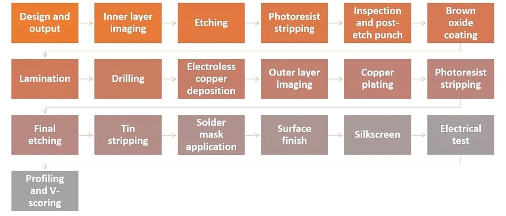
Layering: The chosen material is layered with copper foils. Typically, heavy copper PCBs have copper layers on both sides of the board, which can be pretty thick.
Circuit Design: The PCB layout and design are critical to ensure that the heavy copper traces carry the required current without overheating. Adequate spacing and trace widths must be considered to prevent short circuits and ensure reliable connections.
Laminating: The layered material is laminated under heat and pressure to create a solid board.
Drilling: Precision drilling is done to create holes for components and vias.
Copper Plating: The heavy copper layers are electroplated to increase their thickness. This is a critical step in manufacturing as it defines the copper thickness, a key parameter for heavy copper PCBs.
Etching: Excess copper is etched away to reveal the copper traces and pads according to the PCB design.
Solder Mask Application: A solder mask is applied to insulate and protect the copper traces while exposing the necessary areas for soldering components.
Silkscreen Printing: Component labels, indicators, and other markings are applied.
Surface Finish: The PCB may receive a surface finish like ENIG (Electroless Nickel Immersion Gold) or HASL (Hot Air Solder Leveling) to improve solderability and protect exposed copper.
Advantages of Heavy Copper PCB
✔ High Current Carrying Capacity: These PCBs handle high currents efficiently with thicker copper layers.
✔ Improved Heat Dissipation is essential for power electronics, reducing overheating risks. Enhanced Mechanical Strength is suitable for harsh environments and industrial applications.
✔ Multiple Layer Stacking: Supports complex circuit designs with multilayer heavy copper structures.
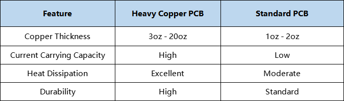
Heavy Copper PCB VS. Standard PCB
Our SSD PCB Case
Previous
Next
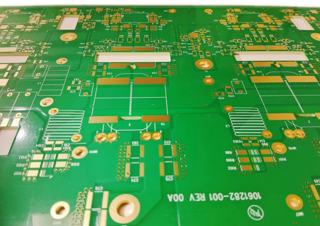
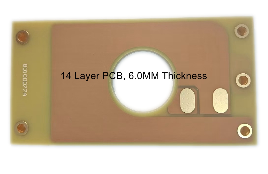
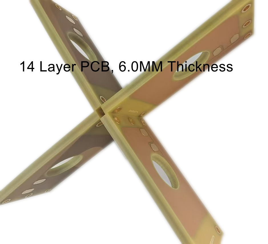
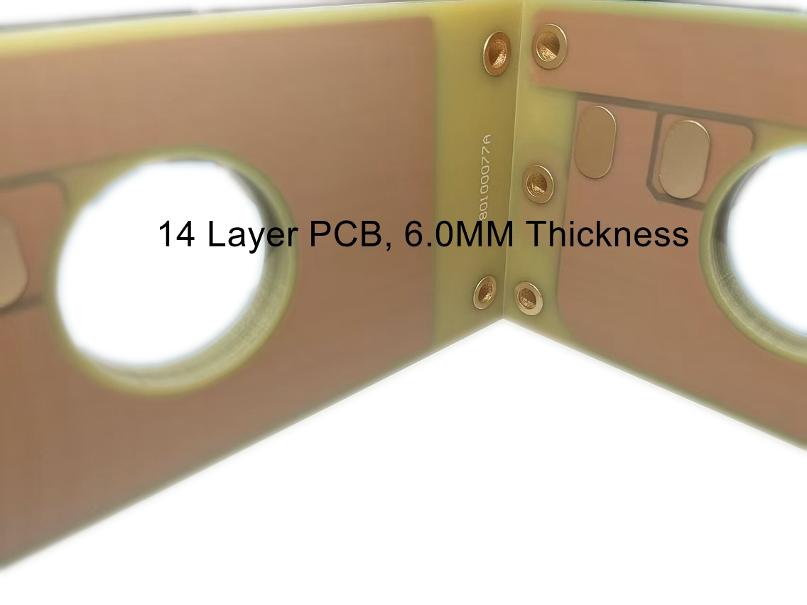
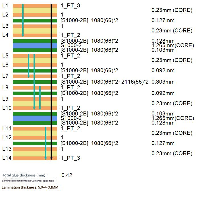
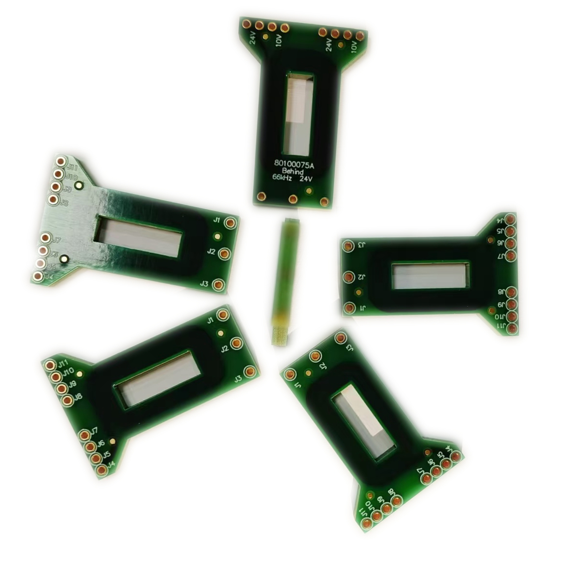
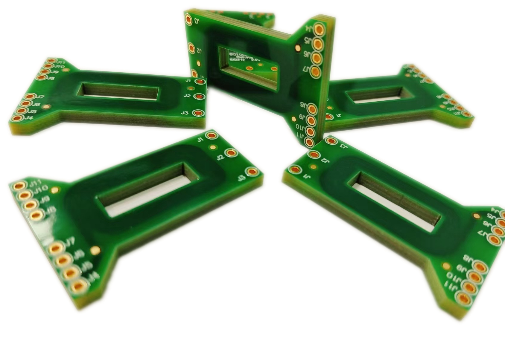
Planar transformer thick copper plate
Planar transformer heavy copper plate’s exceptional craftsmanship:
Number of layers: high-layer board, up to 14 layers
Thick copper: 4OZ
Board thickness: 6.0MM
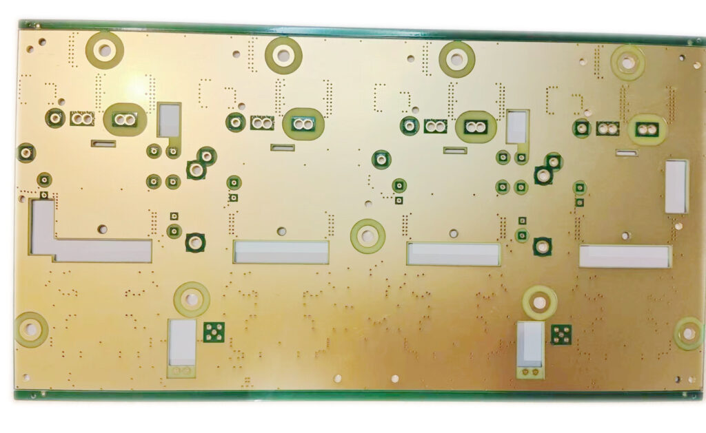
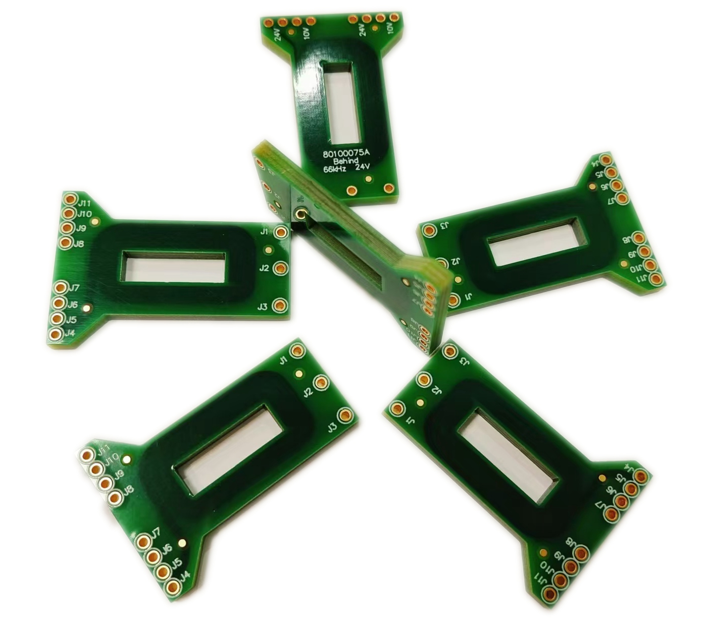
Planar transformer thick copper plate
Planar transformer heavy copper plate’s special craftsmanship:
Number of layers: high-layer board, up to 14 layers
Thick copper: 4OZ
Board thickness: 3.0MM
Previous
Next
Why Choose Us
Competitive Pricing
More than a decade of experience in the PCB industry ensures quality components at competitive prices.
Fast and reliable delivery
Partnership with multiple global logistics providers ensures timely and reliable shipping.
Quality Assurance
A dedicated quality control team conducts manual visual inspections to ensure all products meet strict quality standards.
We have many international certifications:
We also hold several international quality certifications:
At the same time, we are always committed to environmental protection. We have an environmental management system certification to ensure that our manufacturing process is environmentally friendly and sustainable.
Frequently Asked Questions(FAQ)
What is the maximum copper thickness available?
We can manufacture PCBs with up to 20oz copper thickness, depending on design requirements.
Can Heavy Copper PCBs be used in multilayer boards?
Yes, we specialize in multilayer heavy copper designs for complex circuit applications.
How do I get a custom quote?
Contact us with your design files, and our team will provide a competitive quote within 24 hours.
