
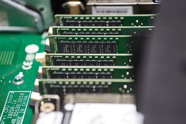
The Benefits of 10 Layer SSD PCB for High-Speed Data Storage
In today’s fast-paced digital world, the demand for high-speed data storage solutions is on the rise, and 10 layer SSD PCBs have become a key component in modern solid-state drive designs. These PCBs offer a variety of benefits that significantly increase data storage and access speeds. In this blog post, we will explore the key benefits of 10 layer SSD PCB and how they contribute to high-speed data storage solutions.
Enhanced Signal Integrity with 10 layer SSD PCB
One of the main benefits of using a 10 layer SSD PCB is the enhanced signal integrity it provides. Signal integrity is critical in high-speed data transmission as it directly affects the SSD’s performance and reliability. The multiple layers in a 10 layer PCB allow for better separation of power and signal lines, minimizing interference and crosstalk.
In a 10 layer design, the arrangement of ground and signal layers can be optimized to reduce electromagnetic interference and improve overall performance. By incorporating a dedicated ground plane, designers can achieve a more stable environment for high-speed signals, which reduces error rates and improves data transmission efficiency. This enhanced signal integrity is essential in applications that require fast data access, such as gaming, video editing, and high-performance computing.
Increased Routing Density with 10 Layer SSD PCB
Using 10 layer SSD PCBs enables greater routing density than traditional 4-layer or 6-layer designs. This increased routing density is essential to accommodate the complex circuitry required for high-speed data storage applications. With more layers available, designers can implement complex routing patterns that efficiently connect various components without sacrificing performance.
This enhanced routing capability enables the integration of advanced technologies, such as faster data buses and more complex controller chips, which are essential to maximizing SSD performance. Additionally, a denser layout can result in a more compact design, allowing manufacturers to create smaller, more efficient SSDs that save space in devices such as laptops, servers, and embedded systems.
Improved Thermal Management Maintains Optimal Operating Temperatures
Effective thermal management is critical for high-speed data storage solutions, as overheating can lead to degraded performance and shortened component life. 10 layer SSD PCBs offer improved thermal management capabilities through better heat dissipation strategies. Multiple layers enable the integration of thermal vias and heat sinks, which help efficiently transfer heat away from critical components.
By incorporating these thermal management features, 10 layer SSD PCBs help maintain optimal operating temperatures, ensuring consistent performance during high-speed data access and transfer. This is especially important in high-workload environments, where applications such as data centres, cloud computing, and gaming demand sustained performance. In addition, enhanced thermal management can extend the life of the SSD, making it a more reliable investment for users.
Enables greater design flexibility
Another significant benefit of 10 layer SSD PCBs is that they offer greater design flexibility. With more layers, engineers and designers can explore innovative layouts that accommodate a variety of components and functions. This flexibility allows for the integration of additional features, such as enhanced power management systems, advanced security features, and support for cutting-edge protocols.
The ability to fine-tune the layout of power and signal traces helps achieve more efficient designs that optimize performance and reliability. For example, designers can easily adjust trace width, spacing, and routing paths to ensure that high-speed signals are transmitted with minimal resistance and interference. This design flexibility is critical to developing next-generation SSDs that meet the evolving needs of consumers and businesses.
Optimize Design for Reduced Power Consumption
Power efficiency is an essential consideration in modern data storage solutions as it directly impacts operating costs and environmental sustainability. 10 layer SSD PCBs can reduce power consumption through improved design and materials. Enhanced routing and signal integrity help minimize the power required for data transmission, thereby reducing overall power consumption.
In addition, the 10 layer SSD PCB’s efficient thermal management capabilities help reduce the need for active cooling solutions, further reducing power consumption. By utilizing energy-efficient components and optimized designs, manufacturers can create SSDs that are not only fast but also consume less power. This is especially important for users of mobile and embedded applications, where battery life and energy efficiency are critical.
Improved Reliability and Durability
Reliability and durability are critical factors when selecting an SSD for high-speed data storage applications. The 10 layer SSD PCB is designed to withstand the rigours of demanding environments, making it a reliable choice for a wide range of applications. The multi-layer structure enhances structural integrity and reduces the risk of damage during manufacturing, assembly, and end-use.
In addition, improved thermal management and signal integrity help improve the SSD’s overall reliability. With less susceptibility to overheating and signal degradation, users can be confident that their data storage solution will operate stably and for a long time. This reliability is critical in mission-critical applications, where data integrity and performance are paramount.
Future-proof to Stay Competitive
As technology advances, the need for faster data storage solutions will only increase. 10 layer SSD PCBs offer a level of future-proofing essential to staying competitive in the fast-paced digital landscape. By supporting higher data rates and advanced technologies, these PCBs enable manufacturers to develop SSDs that can adapt to future trends and requirements.
The 10 layer design’s scalability allows for easy integration of emerging technologies, such as NVMe protocols and next-generation memory chips. This adaptability ensures that users can invest in SSDs that will remain relevant as data storage needs evolve. Ultimately, 10 layer SSD PCBs represent a forward-looking solution that meets today’s needs while meeting tomorrow’s challenges.
10 layer SSD PCB Meet Multiple Needs
10 layer SSD PCBs offer numerous benefits for high-speed data storage solutions, from enhanced signal integrity and increased routing density to improved thermal management and design flexibility. As businesses and consumers continue to seek faster, more reliable data storage options, the advantages of 10 layer SSD PCBs will play a key role in meeting these demands.