
The Evolution of SSD PCB Interfaces: From SATA to NVMe
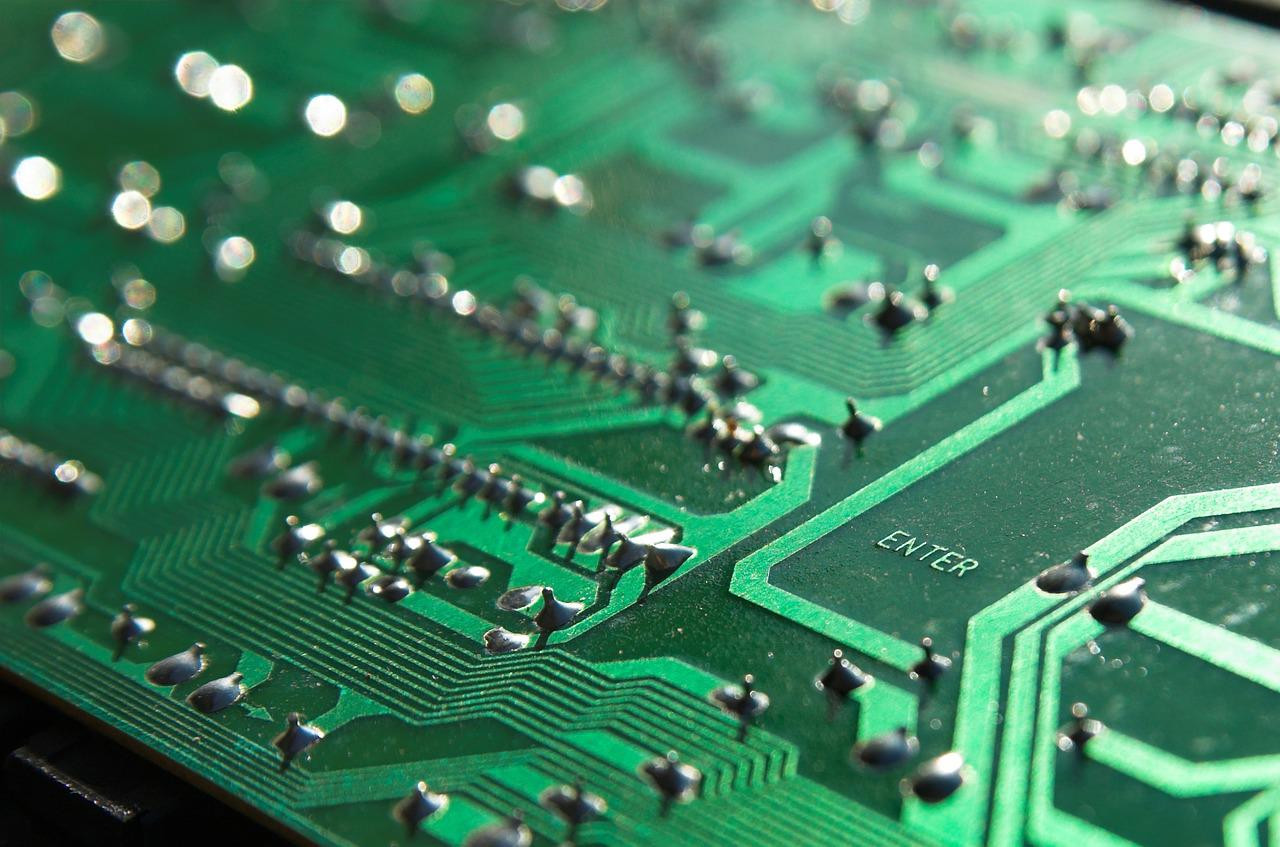
Over the past two decades, SSD PCB architecture has transformed storage technology. Starting with SATA-based designs that mimicked HDD limitations, it rapidly advanced to PCIe and NVMe interfaces that unlocked unprecedented speed and efficiency. This evolution didn’t just boost performance; it redefined how systems access data, powering everything from consumer laptops to enterprise servers. Today’s SSD PCBs are the critical bridge between raw storage and processing power, proving that innovation never stops.
SATA: The Foundation of Modern SSD PCB Design
Serial ATA (SATA) was a critical step in developing SSD PCBs. Introduced primarily for hard drives, SATA provided a reliable way to transition to solid-state storage without requiring dramatic architectural changes. Many early SSD PCBs were built around this interface, benefitting from SATA’s widespread support and simplicity.
However, SATA came with limitations. With theoretical speeds capped at 600MB/s, it couldn’t keep pace with the growing potential of NAND flash. Engineers quickly hit the ceiling. That barrier didn’t just affect raw speed—it limited input/output operations per second (IOPS), energy efficiency, and latency performance. While SATA helped SSD PCBs gain market traction, it also signaled the need for more advanced interfaces.
From Bulky to Portable: The mSATA and Mini PCIe Breakthrough
As mobile computing surged, manufacturers needed smaller SSD PCBs that didn’t compromise performance. mSATA emerged as a compact version of the SATA interface, leveraging a smaller PCB footprint. It fits neatly into ultrabooks and embedded systems while maintaining compatibility with SATA protocols. This shift laid the groundwork for further miniaturization.
In parallel, mini PCIe gained popularity, especially in industrial and specialized computing. While not as fast or widespread as SATA, it allowed SSD PCB integration into unconventional layouts. These form factors enabled new applications but revealed that legacy interfaces wouldn’t suffice for future demands. A breakthrough was imminent.
Data at Warp Speed: The PCIe Advantage
Peripheral Component Interconnect Express (PCIe) marked a revolutionary change. Unlike SATA, PCIe offered multiple lanes for simultaneous data transmission, drastically improving throughput. SSD PCBs built with PCIe interfaces broke past performance bottlenecks—unlocking several gigabytes per second in speed.
This leap wasn’t just about speed. PCIe offered lower latency, greater scalability, and better power efficiency. It also enabled tighter integration between storage and CPU, which is crucial for workloads like video editing, gaming, and cloud operations. PCIe set the stage for a more intelligent, flexible SSD PCB architecture.
Beyond SATA: How NVMe Rewrote the Rules of Storage
While PCIe handled the hardware part, NVMe tackled the software. The Non-Volatile Memory Express (NVMe) protocol was designed from scratch for flash storage. It replaced the outdated command sets of SATA with a streamlined, low-latency instruction path. The result was transformative when SSD PCBs combined PCIe hardware with NVMe logic.
NVMe allowed thousands of queues and parallel requests, dramatically increasing IOPS. It also reduced CPU overhead, optimizing system performance. For enterprise environments, NVMe SSD PCBs delivered unmatched responsiveness. For consumers, it meant near-instantaneous boot times and seamless multitasking. NVMe became the new gold standard in SSD PCB design.
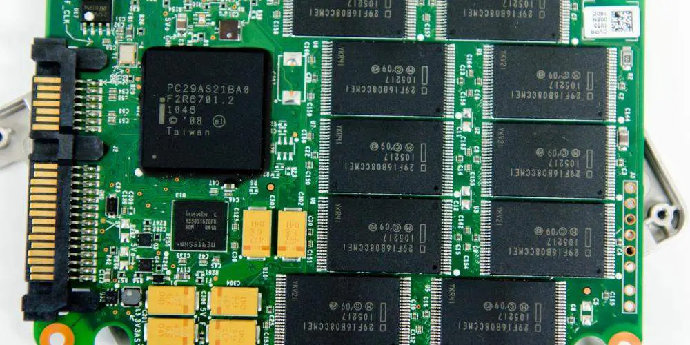
M.2 and U.2 Form Factors: Flexible SSD PCB Integration
New form factors further enhanced the flexibility of SSD PCBs. M.2 SSDs became a favorite among OEMs and PC builders due to their slim profile and high performance. These drives leveraged PCIe and NVMe, fitting directly onto motherboards without cables. M.2 efficiently supported both consumer —and industrial-grade SSD PCB storage solutions
Meanwhile, U.2 catered more to the enterprise space. It offered hot-swap capabilities and robust endurance for server environments. M.2 and U.2 reflected how SSD PCB innovation adapted to speed demands and form factor diversity. These designs helped SSD PCBs infiltrate every corner of modern tech infrastructure.
Speed vs. Temperature: How Modern Storage Stays Cool
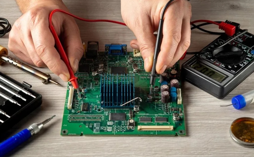
As SSD PCBs got faster, they also got hotter. Managing thermal output became a significant design priority. Engineers introduced heat spreaders, copper layers, and even active cooling solutions. Without effective thermal regulation, performance could be throttled, wasting the benefits of NVMe and PCIe.
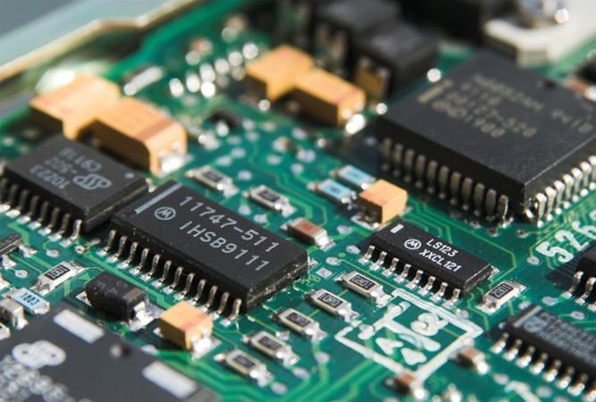
Simultaneously, controller technology advanced. Modern SSD PCB controllers could process parallel requests, self-correct data, and perform onboard encryption. These chips turned SSD PCBs from simple storage devices into intelligent, responsive components. The synergy between thermal design and smart controllers ensured consistent performance under pressure.
Power Efficiency and Durability: The Modern SSD PCB Edge
The latest SSD PCBs are built with power-conscious designs. Thanks to NVMe’s low-latency protocol and modern flash memory, drives now draw less power while delivering more. This shift benefits everything from battery-powered laptops to energy-sensitive data centers.
Durability has also improved. Wear-leveling algorithms, over-provisioning, and high-endurance NAND flash all contribute to longer SSD PCB lifespans. Today’s designs are also more reliable, resilient, and environmentally friendly than ever before. These gains help businesses cut long-term costs and reduce electronic waste.
SSD PCB Interfaces Drive the Future of Storage
The evolution of SSD PCB interfaces, from SATA to NVMe, has been revolutionary. These changes didn’t just affect speed—they redefined what modern SSD PCBs can do. As data demands grow, these components must keep innovating. Interfaces will continue evolving, pushing speed, efficiency, and intelligence boundaries.