
What are the benefits of using 2 layer 1OZ PCB in IoT devices?
As the Internet of Things revolutionizes various industries, the demand for reliable and efficient hardware components has also risen sharply. In addition to software technology, the PCB is another critical component in IoT devices. Among the different types of PCBs available, 2 layer 1OZ PCB offer unique advantages. In this guide, we will take a deep dive into the benefits of using 2 layer 1OZ PCB in IoT devices and explore why this choice can improve your IoT projects’ reliability and performance.
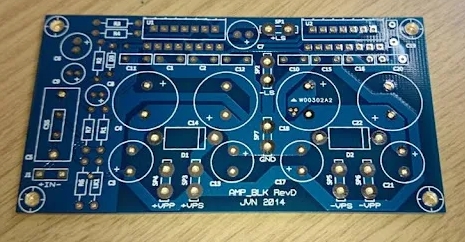
Durability unreliability of 2 layer 1OZ PCB
One of the main advantages of using 2-layer 1OZ PCBs in IoT devices is their enhanced durability and reliability. The 1-ounce copper thickness in these PCBs ensures a sturdy structure that can withstand various environmental conditions and mechanical stresses. This is very important for IoT devices operating in diverse and sometimes harsh environments. The increased copper thickness provides better current carrying capacity and heat dissipation, reducing the risk of overheating and extending the life of the device. In addition, the additional layers in the 2-layer design allow for more complex circuits, resulting in more reliable and stable connections, which is crucial for the consistent performance of IoT devices.
Improved Performance and Signal Integrity of 2-Layer 1OZ PCBs
Performance and signal integrity are critical for IoT devices, as data transfer and processing must be seamless and accurate. 2 Layer 1OZ PCB designs have distinct advantages. Their extra layers allow for better signal and ground layer separation, reducing EMI and crosstalk between traces. This results in more precise signals and improved device performance. The 1-ounce copper thickness also helps reduce resistance and enhance conductivity, ensuring efficient power delivery and signal transmission. This is very important for IoT devices requiring stable, high-speed data communications.
More Flexible Design and More Convenient Customization
IoT devices come in various shapes, sizes, and functions, requiring flexible and customizable PCBs to meet these needs. 2-Layer 1OZ PCBs offer high flexibility in design and customization. Extra layers provide more routing space, enabling designers to achieve more complex and compact designs. This is especially beneficial for some IoT devices that need to be small and lightweight while maintaining high functionality. 1-ounce copper thickness supports various design requirements, such as higher current carrying capacity and better thermal management. This design flexibility ensures that IoT devices can be tailored to specific applications and user needs, enhancing their functionality and market appeal.

Features Enhanced Thermal Management
Thermal management is a critical aspect of IoT device design, as overheating can lead to device failure and performance degradation. 2-layer 1OZ PCBs excel in thermal management due to their increased copper thickness. The 1-ounce copper layer effectively dissipates heat generated by components, preventing hot spots and ensuring even temperature distribution across the PCB. This is especially important for IoT devices that operate continuously or in high-temperature environments. Enhanced thermal management directly contributes to the reliability and lifespan of IoT devices. By preventing overheating and thermal cycling, our PCBs reduce the risk of component degradation and failure.
Simplifies Prototyping and Testing
Prototyping and testing are essential steps in IoT device development, and the simplicity of 2-layer 1OZ PCBs aids these processes. The simplicity of design and manufacturing of 2-layer PCBs makes it easier to produce prototypes quickly and efficiently. At the same time, the 1-ounce copper thickness ensures that prototypes have the same electrical and thermal properties as the final product, allowing for accurate testing and validation. This simplifies the iteration process, thereby shortening the development cycle and time to market for IoT devices. The ease of using them for prototyping and testing helps manufacturers improve their designs and ensure that the final product meets all performance and reliability standards.
Achieving IoT Success
2-layer 1OZ PCBs offer numerous advantages that make them an ideal choice for IoT devices. Their enhanced durability, improved performance, design flexibility, thermal management, and ease of prototyping and testing provide a comprehensive solution for IoT device manufacturers. By leveraging the benefits of 2-layer 1OZ PCBs, you can ensure that your IoT devices deliver reliable performance, withstand harsh environments, and meet the needs of your customers.