
What are the benefits of using a 2 layer HAL PCB in IoT devices?
IoT devices are changing the way we live, bringing connectivity and smart features to a wide range of devices. At the heart of these are 2 layer HAL PCB. These PCBs are essential for their efficiency, cost-effectiveness, and adaptability in IoT applications. In this guide, we take a deep dive into the many benefits of using 2-layer HAL PCBs in IoT devices.
Cost-Effectiveness and Economic Benefits of 2 Layer HAL PCB
Cost is a key factor in the production and scalability of IoT devices, and 2-layer HAL PCBs offer significant economic advantages. Their manufacturing process is simpler and less resource-intensive than multi-layer PCBs. This simplicity translates to lower production costs. Prototyping is an essential stage in the development of IoT devices. 2-layer HAL PCBs are affordable and can produce multiple prototype iterations without excessive costs. This flexibility allows engineers to try out different designs and features, ultimately creating a more refined and reliable end product.
Enhanced Durability and Reliability of 2 layer HAL PCB
Durability and reliability are critical for IoT devices, and the HAL process in 2-layer HAL PCBs ensures that the solder joints on the PCB are strong and uniform. This makes for a stronger bond between components and the board, reducing the risk of mechanical failure. Enhanced solder joint strength is particularly beneficial for IoT devices that may experience vibration, shock, or temperature fluctuations during operation. The HAL treatment forms a protective layer of solder on the copper traces that helps prevent oxidation and corrosion. This protection is critical for IoT devices deployed in harsh or outdoor environments.
Simplified Design and Layout
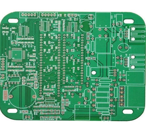
The design and layout of PCBs have a significant impact on the functionality and performance of IoT devices, and 2 layer HAL PCBs have only two layers, providing ample space for signal routing while maintaining a simple layout. This efficient space utilization is critical for compact IoT devices, so designers can implement necessary functions without overcrowding the board, which can avoid signal interference and other issues. A simpler layout makes it easier to diagnose and fix problems during the prototyping and production stages. Engineers can quickly identify and resolve potential issues, speeding up the development process and ensuring that the final product meets quality standards.
Optimal Performance and Functionality
Performance is a key consideration for IoT devices, as they need to operate efficiently and reliably under a wide range of conditions. The uniform solder layer provided by the HAL process ensures consistent electrical performance. This stability is critical to the reliable operation of IoT devices, which rely on precise signal transmission and minimal interference. The consistent electrical performance of 2-layer HAL PCBs helps improve the overall reliability and effectiveness of IoT solutions. At the same time, their dual-layer design allows for flexible placement of components, enabling designers to optimize layouts for performance and functionality. This flexibility is especially important for IoT devices that may need to integrate a variety of sensors, communication modules, and other components.
Performance Benefits of 2-layer HAL PCBs
The performance of IoT devices is largely affected by the quality and characteristics of 2-layer HAL PCBs. The two conductive layers in a double-layer PCB provide ample routing options for electrical signals, reducing the possibility of signal interference and crosstalk. This improves signal integrity, which is critical to the reliable operation of IoT devices. Enhanced signal integrity ensures accurate data transmission and processing, which helps improve the overall performance of the device. And effective thermal management can maintain the performance of electronic components. The HAL process enhances the thermal conductivity of the PCB by providing a uniform solder coating, thereby promoting efficient heat dissipation.
Value in IoT Devices
2-layer HAL PCBs provide many benefits to IoT devices, including cost-effectiveness, reliability, design flexibility, performance, and more. By choosing 2-layer HAL PCBs, IoT devices can improve their quality and competitiveness while being able to meet market demands.