
What are the common sizes for 2 layer TG170 PCB?
In electronics, PCBs are the backbone of most modern devices. Among the various types of PCBs, TG170 PCBs are designed to handle higher temperatures, which is crucial in applications that require robust thermal management. In this guide, we’ll deeply dive into the common sizes of 2 layer TG170 PCB, providing valuable insights for those needing these essential PCBs. We’ll explore their applications, benefits, and the importance of choosing the right size for your project.
Standard Sizes of 2 layer TG170 PCB
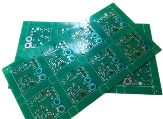
When discussing the common sizes of 2-layer TG170 PCBs, their “size” can refer to both the board’s physical dimensions and the layers’ thickness. Standard sizes are generally based on industry specifications to accommodate various applications and manufacturing processes. The most common sizes include 18×24 inches, 24×36 inches, and 36×48 inches. These sizes are generally chosen to optimize material usage and reduce waste during the production process. The standard thickness of a 2-layer PCB generally ranges from 1.6mm to 3.2mm, with 1.6mm being the most common due to its combination of durability and flexibility. However, the thickness can be customized to meet specific application needs, especially in environments requiring enhanced mechanical strength or specific electrical performance.
Customized 2 layer TG170 PCB Sizes and Their Applications
While standard sizes are the most popular, customized-sized 2-layer TG170 PCBs are equally important, especially for specialized applications. Customized PCBs are designed to meet unique requirements that standard sizes cannot meet. For example, in industries such as aerospace and automotive, custom-sized 2-layer TG170 PCBs ensure optimal performance and integration. This customization process allows for greater design flexibility and can significantly improve the functionality and reliability of the end product. Additionally, customized PCBs can help reduce the device’s overall weight, which is critical for applications such as drones and portable electronics.
Benefits of Using 2 layer TG170 PCB
The advantages of using 2-layer TG170 PCBs are numerous. First, they have excellent thermal stability, which is ideal for high-temperature environments. This is particularly beneficial for automotive and industrial automation, where components are exposed to high temperatures for long periods of time. Secondly, 2-layer TG170 PCBs have better electrical properties due to their higher glass transition temperature (TG). This ensures that the electrical performance of the PCB remains stable even under thermal stress, which is critical for maintaining signal integrity in high-speed circuits. In addition, they enable more complex circuit designs, allowing more components and functions to be integrated in a smaller footprint.
Small Size
Small-size 2-layer TG170 PCBs are essential for modern electronic devices, focusing on compactness and portability. Common sizes in this category include 1×1 inch, 2×2 inch, and 2×4 inch. These smaller PCBs are ideal for wearable technology, portable medical devices, and more applications. The main advantage of 2-layer TG170 PCBs is their ability to fit into small spaces without compromising performance. However, designing and manufacturing these boards requires careful consideration of signal integrity, heat dissipation, and component density. Advanced manufacturing techniques such as SMT and microvias are often used to maximize the functionality of small PCBs.
Large Sizes
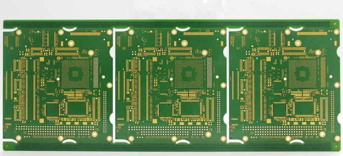
On the other hand, large 2-layer TG170 PCBs are used for applications that require large circuits and high power handling capabilities. Common sizes in this category include 12×12 inches, 18×24 inches, and even larger custom sizes. They are often used in industrial control systems, large communication networks, and high-performance computing systems. Their main advantage is accommodating more components and complex circuit designs. This allows multiple functions to be integrated onto a single board, reducing interconnect requirements and improving overall system reliability.
High-Density Interconnect (HDI)
High-Density Interconnect (HDI) 2-layer TG170 PCBs are designed to accommodate a higher density of components and interconnect within a given area. Common sizes include 4×4 inches, 6×6 inches, and 8×8 inches. These sizes were chosen to balance the need for compactness with the need for extensive functionality. They also feature micro vias, blind and buried vias, and fine-line traces to improve electrical performance. They are used in advanced applications such as smartphones, tablets, and other high-performance consumer electronics. Using HDI technology enables designers to create more complex and powerful devices without increasing size.
Choosing the Right Size
You need to choose the right size PCB based on the specific requirements of different applications, the available space within the device, and the performance characteristics required. Standard sizes provide convenience and cost-effectiveness, while custom sizes provide tailored solutions for unique challenges. Small size PCBs are ideal for compact devices, while large size PCBs excel in applications that require a large amount of circuitry.