
What are the design rules for 3 OZ PCB?
PCBs are the backbone of all electronic devices, and for applications that require higher current capacity and enhanced thermal management, 3 OZ PCB is the preferred choice. These PCBs use thicker copper layers to provide better performance in complex environments. However, designing 3 OZ PCBs comes with its challenges and rules that must be strictly followed to ensure reliability and efficiency. This article will introduce you to the key design rules for 3 OZ PCBs and provide some insights and best practices.
Basics of 3 OZ PCB Design
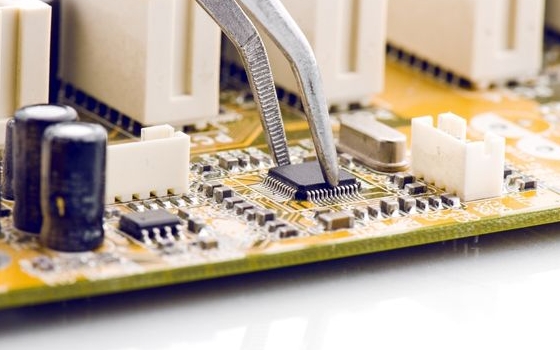
“3 OZ PCB” refers to the thickness of the copper layer used in the PCB, measured in ounces per square foot. The copper thickness of 3 OZ PCBs is approximately 105 microns, which is three times thicker than the standard 1 OZ copper used in most PCBs. This increased thickness allows for higher current carrying capacity and better heat dissipation, making it ideal for power electronics, automotive, and industrial applications. When designing 3 OZ PCBs, we use thicker copper that requires wider traces and more spacing to accommodate higher currents and avoid overheating. The increased thickness also affects the etching process, requiring adjustments during manufacturing to ensure precise and reliable results.
Material Selection for 3 OZ PCB
Choosing the right material is a fundamental step in designing a 3 OZ PCB. The substrate material chosen must be able to withstand the higher thermal and electrical loads brought by thicker copper layers. For applications that generate a lot of heat, we use high-temperature substrates or substrates with enhanced thermal conductivity. In addition, the selection of solder mask and surface treatment will also meet the performance requirements of 3 OZ PCB. In addition, the dielectric material between copper layers also plays a key role in maintaining signal integrity and thermal performance. For high-power applications, materials with lower dielectric loss and higher thermal stability are our first choice.
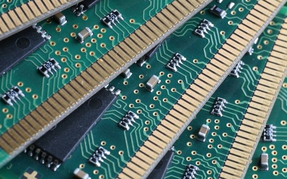
Trace Width and Spacing
One of the most critical aspects in designing a 3 OZ PCB is determining the appropriate trace width and spacing. Thicker copper layers increase the current-carrying capacity of the trace but also require wider traces to prevent overheating and potential failures. For 3 OZ PCBs, the trace width needs to be much wider than a standard 1 OZ PCB at the same current. Therefore, we increase the spacing between traces to prevent electrical shorts and ensure proper insulation. This is especially important in high-voltage applications, as increased spacing helps avoid arcing and maintain safety.
Thermal Management in Design
Since thicker copper layers generate higher currents and heat, we add more effective thermal management in our designs. Adequate heat dissipation prevents overheating, ensures reliability, and prolongs the life of the PCB. We manage heat in 3 OZ PCBs through several strategies, such as using thermal vias, heat sinks, and optimizing board layout. Conductive material fills small holes called thermal vias, which connect the top and bottom layers of the PCB, allowing heat to dissipate more effectively.
Strategically placing thermal vias around heat-generating components can significantly improve thermal performance. Additionally, using heat sinks and thermal pads can help manage heat dissipation from high-power components.

Via Design and Plating
Vias are an integral part of PCB design and are used to provide electrical connections between different layers of the board. In 3 OZ PCBs, due to the increased copper thickness, special care is taken when designing and plating vias. Some thicker copper layers use thicker walls to ensure reliable electrical connections and structural integrity. The plating process for through-holes in 3 OZ PCBs also caters to sufficient copper deposition to handle higher current and thermal loads. Via reliability can be improved by using techniques such as filling or back drilling, especially in high-density designs.
Ultimately
We consider a variety of factors when designing 3 OZ PCBs, from material selection and trace width to thermal management and signal integrity. We create PCBs that provide superior performance and reliability in high-current applications. Working with us ensures that your design is manufacturable and meets all necessary specifications.