
What are the unique design considerations for 6 layer SSD PCB?
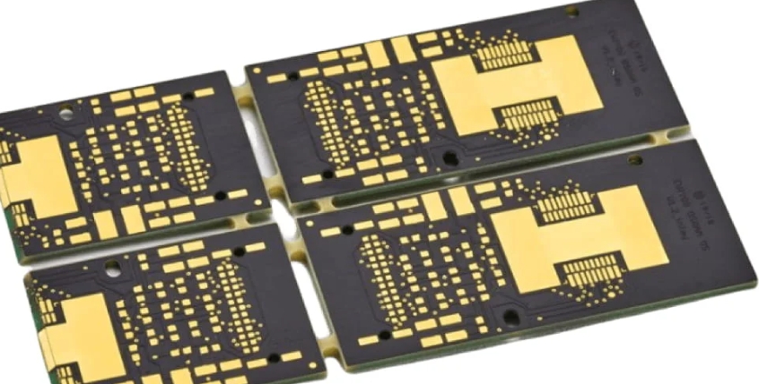
SSDs are the most critical components in modern computers, providing high-speed data storage and retrieval. The performance and reliability of SSDs are greatly affected by their PCB design. For wholesalers looking to source 6-layer SSD PCBs, knowing the unique design factors is critical to ensuring product quality and performance. This guide provides a comprehensive guide that takes a deep dive into the unique design aspects of 6 layer SSD PCB.
6-layer SSD PCB Layer Stackup and Signal Integrity Design
One of the primary considerations when designing a 6 layer SSD PCB is the layer stackup. This configuration can significantly affect signal integrity, critical for high-speed data transmission. Typically, a 6-layer PCB stack-up may include:
Top layer: used for high-speed signal routing and component placement.
Ground layer: provides a reference ground for signals, reduces noise, and improves signal integrity.
Power layer: distributes power to various components while minimizing voltage drops and electromagnetic interference (EMI).
Inner signal layer: used to route critical signals that must be shielded from external noise.
Ground plane: another ground plane that further enhances signal integrity.
Bottom Layer: Additional Signal Routing and Component Placement.
This arrangement helps minimize electromagnetic interference (EMI) and crosstalk, ensuring stable and reliable signal transmission. Our 6 layer SSD PCBs feature a controlled impedance trace design to ensure signal integrity. This involves precise calculations and manufacturing processes to maintain consistent impedance, reduce signal reflections, and ensure reliable data transmission. Crosstalk between adjacent traces can severely degrade signal quality. Our designs employ various techniques, such as increasing spacing between critical signal traces.

Power Distribution and Ground Plane of 6 layer SSD PCB
Effective power distribution is critical to the stable operation of SSD PCB, and SSD requires stable and clean power to operate reliably. In a 6-layer SSD PCB, the power plane is carefully designed to provide efficient power distribution. Usually, the power plane is located in the middle layer of the PCB to reduce noise coupling and ensure a uniform power supply across the board. The power plane must be designed to minimize voltage drop and maintain a stable voltage level. We use wider traces and planes to reduce resistance. In addition, we will place decoupling capacitors close to the IC power pins to help filter out noise and stabilize the power supply.
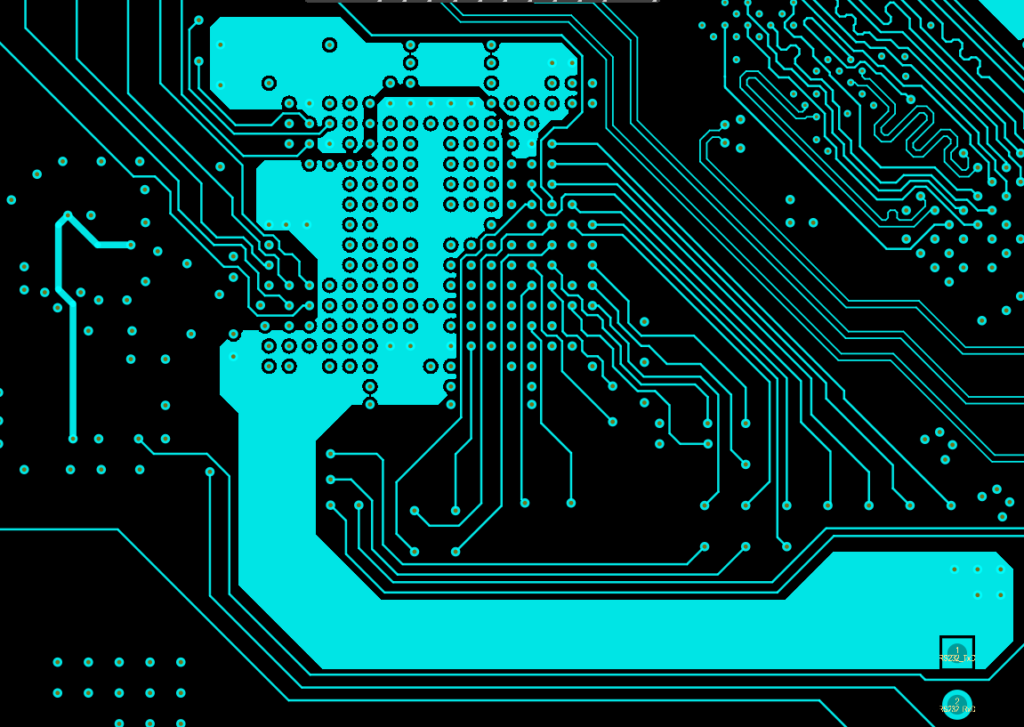
As a reference for the signal, the ground plane plays a vital role in reducing noise and ensuring signal integrity: in a 6-layer PCB, it is best to have at least two dedicated ground planes. These planes provide a reliable reference for all signals and help reduce EMI by shielding and controlling noise within the PCB. The ground plane should be adjacent to the signal layer to form a controlled impedance environment. This proximity helps maintain signal integrity by reducing crosstalk and signal reflections.
Thermal Management Strategy
Because SSD components have high power density and heat generation, thermal management is essential for any SSD PCB design. An effective thermal management strategy can help them dissipate heat effectively. We use high thermal conductivity materials as PCB substrates, such as polyimide or high-grade FR-4, to help dissipate heat more effectively. This choice ensures that heat is evenly distributed across the board, reducing hot spots. Thicker copper layers are also used to enhance heat dissipation. We use 1 ounce or even 2 ounces of copper for power and ground planes to improve thermal performance. At the same time, we also add thermal vias between layers to enhance heat transfer from surface components to inner layers. These vias create a path for heat to move away from hot spots, making it more evenly distributed on the PCB.
High-speed data signal design
The routing of high-speed data signals is another unique consideration in the 6-layer SSD PCB design. Proper routing techniques are critical to minimize signal loss and ensure data integrity. We use a strong PDN, and a stable PDN is critical for high-speed operation. We design power and ground planes to provide low-impedance paths, reduce noise, and ensure consistent power delivery to high-speed components. Strategically placed decoupling capacitors near high-speed ICs filter power supply noise and provide local energy storage. This helps maintain signal integrity by preventing power supply fluctuations from affecting high-speed signals. For high-speed differential pairs, length matching is critical to ensure that the signal pairs arrive at the receiver at the same time. We use precise length-matching techniques to minimize skew and maintain signal integrity.

Material selection and reliability
The material selection of a 6-layer SSD PCB can significantly affect its performance and reliability. High-frequency laminates and low-loss materials are often used to support the high-speed operation of SSDs. We select low-loss dielectric materials to reduce signal attenuation and maintain high-frequency signal integrity. Materials with a low dielectric constant (Dk) and dissipation factor (Df) support high-speed data transmission and minimize losses. High-quality solder mask and silkscreen layer materials are also used to protect the 6-layer SSD PCB surface and provide clear and easy-to-read markings. These materials resist thermal degradation and chemical corrosion, helping to extend the overall life of the PCB. We select materials with high tensile strength and flexibility to ensure the mechanical robustness of the 6-layer SSD PCB. This prevents cracking and delamination under mechanical stress.
Ultimately
The design considerations for 6-layer SSD PCBs are multifaceted and include layer stacking, power distribution, thermal management, high-speed data routing, material selection, and more. For wholesalers looking to source these PCBs, understanding these design aspects is critical to ensuring the performance, reliability, and lifespan of the SSD.