What is a 2 Layer Red Solder Mask PCB?
The previous article introduced the advantages of a 2-layer green solder mask PCB. Today, we follow the theme and share with you what a 2 layer red solder mask PCB is, clarifying the definition of a 2-layer red solder mask PCB and its role in shaping modern electronic equipment.
Learn about 2-Layer Red Solder Mask PCB
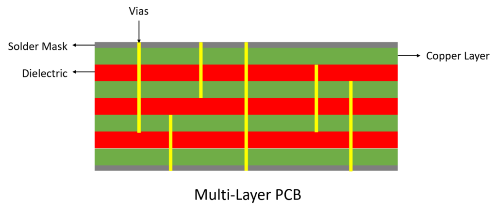
A 2 layer PCB is a circuit board with conductive traces and components on the top and bottom layers. These layers are typically made from the substrate material and provide mechanical support for the circuit board. Copper foil is laminated to these layers to form conductive pathways that connect various electronic components.
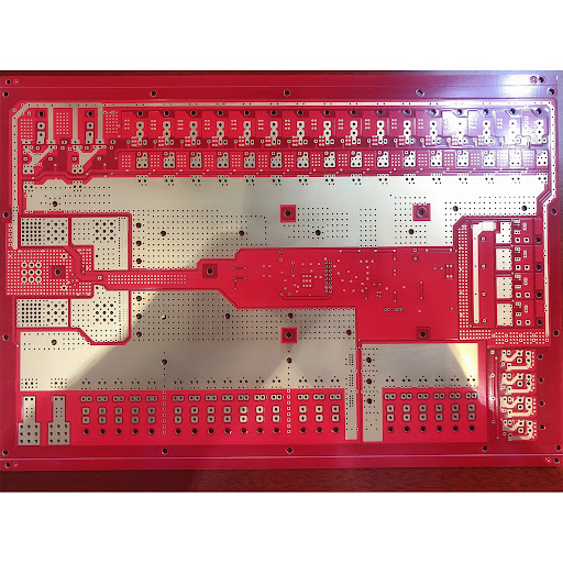
A red solder mask means solder mask is a layer of polymer that is applied to the conductive traces, leaving only the component pads exposed. It prevents solder bridges between closely spaced traces, protects against environmental factors such as moisture and dust, and improves the overall aesthetics of the board. We used a screen printing process to apply the red solder mask. The process involves applying a layer of liquid solder mask material to the surface of the PCB and then curing it under UV light. The areas not covered by the solder mask are then exposed for component placement and soldering.

Why is the 2 layer red solder mask PCB red?
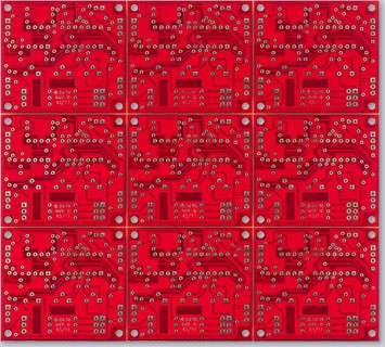
Choosing red for the solder mask on a 2-layer PCB is primarily a design preference rather than a functional requirement. The color of the solder mask has no direct impact on the electrical performance or functionality of the PCB. Additionally, the red color enhances the contrast between the solder mask and the metal traces and components on the PCB, making visual inspection easier during manufacturing and assembly. Some manufacturers and designers also choose red to make their products stand out or to align with a specific color scheme.
2 layers of red solder mask PCB layers, materials, etc.
They consist of two main layers, the top and bottom, providing mechanical support for the circuit board. Conductive paths are formed by laminating copper foil to the base layer. These traces include circuits and connect various electronic components on the PCB. The red solder mask is the protective layer applied to the conductive traces. Typically made of a polymer material, it insulates traces and prevents accidental electrical connections during soldering. Solder mask also protects the PCB from environmental factors such as moisture, dust, and more. 2-layer red solder mask PCBs often include a screen-printed layer for labeling and labeling components. This layer is applied over the solder mask and contains symbols, component designators, and other markings to aid assembly and troubleshooting. The manufacturing process involves substrate preparation, copper layer deposition, circuit pattern etching, solder mask application, and component assembly.

Highlights of applications in different industries
Their application in different industries has significant highlights. In addition, red solder resist materials generally have high heat resistance, ensuring that PCBs can withstand high temperatures during various processes, including soldering. This property helps improve PCBs’ overall reliability and durability in multiple applications. In addition, the red solder mask enhances the contrast of component placement and solder joints, thereby increasing the accuracy of the assembly process. This primarily benefits complex circuits and small electronic components, such as telecommunications, automotive, and consumer electronics. This versatility makes them suitable for various industries, from industrial automation to medical equipment.
Design efficiently
There are several key factors to consider when designing an efficient 2-layer red solder mask PCB. Firstly, selecting components and their placement on the board is critical. Compact and organized layout to minimize signal interference and maintain signal integrity. Efficient power distribution and adequate copper traces on the PCB help reduce voltage drops and ensure stable power delivery to components. A ground plane can enhance signal integrity and minimize electromagnetic interference (EMI). Consider PCB design manufacturability. Optimized to simplify assembly and inspection by maintaining adequate clearance between components, proper spacing, and consistency with industry-standard manufacturing processes.
At last
From this, we can learn about 2-layer red solder mask PCB related information in this article. This guide gives users and consumers a deeper understanding of their importance in the entire PCB industry. As technology continues to advance and more diverse industries are created, they will be able to play a vital role.

