What is an HDI PCB and how does it differ from traditional PCB?
HDI PCB, the pinnacle of modern electronic design, exudes confidence with its unparalleled performance and adaptability to meet the needs of advanced devices. As the industry gravitates towards compact and feature-rich products, the role of HDI PCBs becomes indispensable and a symbol of high performance. Unlike traditional PCBs, HDI PCBs are characterized by their complex designs, smaller features, and enhanced interconnection density, enabling the development of high-performance electronic solutions in a compact space. Next, we will introduce you to HDI PCBs’ definitions, characteristics, and applications, instilling confidence in their capabilities and why the industry is increasingly adopting HDI technology.
A Comprehensive Overview of HDI PCB
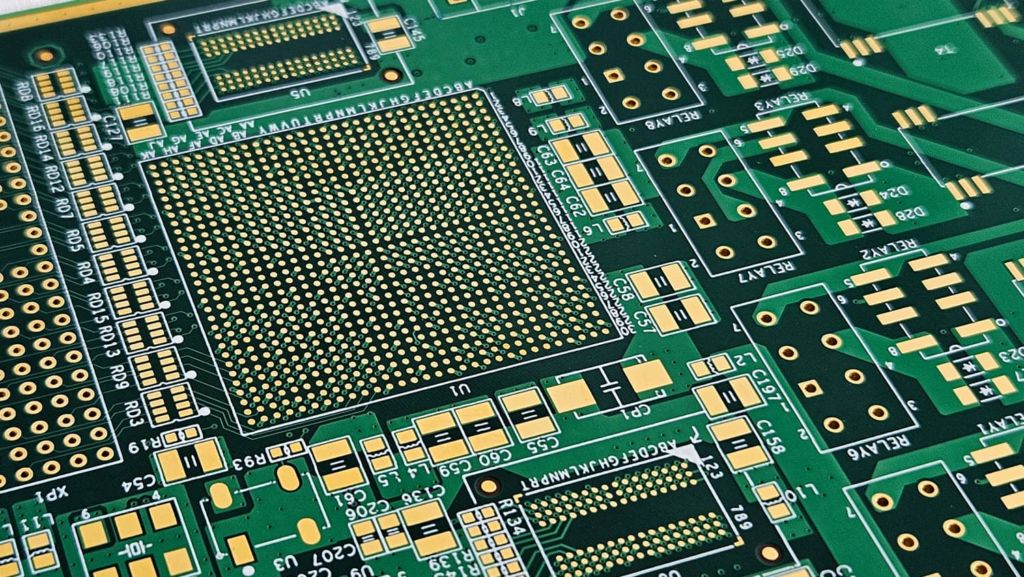
HDI PCBs are distinguished by their ability to support dense wiring within a small area. This is achieved through advanced features such as micro vias, blind vias, buried vias, and thin traces. These features enable higher functionality on smaller boards, catering to industries prioritizing space-saving designs and cutting-edge performance.
One of the defining aspects of HDI PCBs is their material composition. HDI boards often use high-temperature laminates, low-loss materials, and thinner copper layers to accommodate the demands of high-speed and high-frequency signals. Additionally, HDI PCBs leverage advanced manufacturing techniques like sequential lamination and laser drilling to achieve their compact and efficient designs.
For example, HDI PCBs can feature traces as narrow as 0.075mm and vias as small as 0.1mm, enabling them to house components with high pin counts. This contrasts with traditional PCBs, which often focus on simplicity and cost-effectiveness for less complex applications.

Key Features and Characteristics of HDI PCB
The unique features of HDI PCBs set them apart from their traditional counterparts. One of the most significant differences is that manufacturers use microvias, tiny holes drilled into the PCB, to connect its various layers. Microvias allow for higher layer-to-layer connectivity, which is essential for high-density designs.
Another hallmark of HDI PCBs is the utilization of buried and blind vias. Unlike through-hole vias in traditional PCBs, these specialized vias do not pass through the entire board, maximizing the space for routing and components. Moreover, HDI PCBs often incorporate stacked or staggered vias for further optimization.
Signal integrity is another area where HDI PCBs excel. With shorter signal paths and reduced parasitic effects, HDI boards ensure minimal signal loss and crosstalk, making them ideal for high-speed applications. This contrasts with traditional PCBs, which may struggle to maintain signal quality in complex designs due to longer signal paths and increased parasitic effects.
Differences between it and traditional PCB
The most noticeable difference between HDI and traditional PCBs is their design and manufacturing complexity. Traditional PCBs typically have fewer layers, larger traces, and through-hole vias, making them suitable for basic applications. In contrast, HDI PCBs cater to sophisticated requirements with multiple layers, fine features, and advanced technology.
The production of HDI PCBs involves state-of-the-art equipment and processes, including laser drilling and sequential lamination. These techniques allow for precise construction but also contribute to the higher cost of HDI boards. However, the benefits often outweigh the costs, especially in applications with critical performance and compactness.
For example, a traditional PCB may support devices with larger footprints and lower density, such as household appliances. On the other hand, manufacturers use HDI PCBs in smartphones, tablets, and automotive systems, where space constraints and functionality are paramount.

Its Applications in Various Industries
HDI PCBs are a cornerstone of modern electronic innovation, finding applications in various industries. In the consumer electronics sector, HDI PCBs are integral to the design of smartphones, laptops, and wearable devices. Their compact size and high functionality enable the seamless integration of advanced features into small form factors.
The automotive industry also benefits from HDI PCBs, particularly advanced driver-assistance systems (ADAS), infotainment systems, and battery management systems (BMS). These applications demand reliable and high-performance PCBs, which HDI technology delivers.
Telecommunications is another field where HDI PCBs play a pivotal role. With the rise of 5G and high-speed networking, the need for PCBs that can handle high-frequency signals and dense layouts has never been greater. HDI PCBs are at the forefront of enabling these technologies, making them indispensable in industries like aerospace, medical devices, and industrial automation.
Real-World Examples of HDI PCB Integration
The adoption of HDI PCBs in real-world applications underscores their versatility and value. For instance, Apple’s iPhones use HDI technology to incorporate high-performance components within a slim and lightweight design, enabling the brand to maintain its reputation for delivering cutting-edge devices.
Tesla uses HDI PCBs in its electric vehicles to efficiently manage power and data flow in the automotive world. The compact and robust nature of HDI PCBs aligns with the needs of electric cars, where space and reliability are crucial.
According to market research, the global demand for HDI PCBs is projected to grow significantly in the coming years. This growth is driven by technological advancements that require more compact and high-performance PCBs and increasing consumer expectations for feature-rich products that can only be achieved with HDI technology.

Investment Advantages as well as Competitiveness
The benefits of HDI PCBs extend beyond their compact design and high functionality. By reducing the required layers and optimizing material use, HDI PCBs can contribute to long-term cost savings, providing a reassuring return on investment. Additionally, their superior thermal management ensures reliable operation even in demanding environments.
For businesses, investing in HDI PCBs can lead to greater innovation and Competitiveness. Whether enabling IoT connectivity, improving signal performance, or supporting complex designs, HDI technology offers a pathway to meeting the challenges of modern electronic design.
HDI PCBs are the first choice for businesses
HDI PCBs represent a significant leap forward in PCB technology, offering unparalleled performance and adaptability for modern electronics. Their advanced features, compact designs, and superior signal integrity make them the go-to choice for industries prioritizing innovation and efficiency.

