What is the maximum data transfer rate achievable with a 6 layer SSD PCB?
Solid-state drives have become the storage solution of choice in an ever-evolving technology landscape, especially in high-performance applications. The printed circuit board is at the heart of SSD technology and is crucial in determining performance characteristics such as data transfer rates. This blog post takes a deep dive into the maximum data transfer rates achievable with a 6 Layer SSD PCB, providing users with critical insights into this vital component of modern computing.
Introduction to 6 Layer SSD PCB
A 6 Layer SSD PCB is a sophisticated electronic board that provides the necessary infrastructure for SSDs. Comprising 6 layers of interconnected circuitry, these PCBs offer enhanced signal integrity, improved thermal management, and the ability to accommodate complex routing needed for high-speed data transfer. As data demands continue to rise, understanding the capabilities of a 6 layer SSD PCB is crucial for users seeking efficient and reliable storage solutions. This introduction highlights the importance of data transfer rates in SSD applications and sets the stage for a deeper exploration of what users can expect from a 6 layer SSD PCB.
The maximum data transfer rate of a 6 layer SSD PCB is influenced by various factors, including the design of the PCB, the type of NAND flash memory used, and the interface protocol employed. Most modern SSDs utilize NVMe (Non-Volatile Memory Express) interfaces, significantly enhancing data transfer rates compared to traditional SATA interfaces. With the proper configuration and optimization, 6 layer SSD PCBs can achieve impressive data transfer rates, making them suitable for applications requiring high-speed data access, such as gaming, video editing, and large-scale data analytics.
Factors that affect data transfer rates
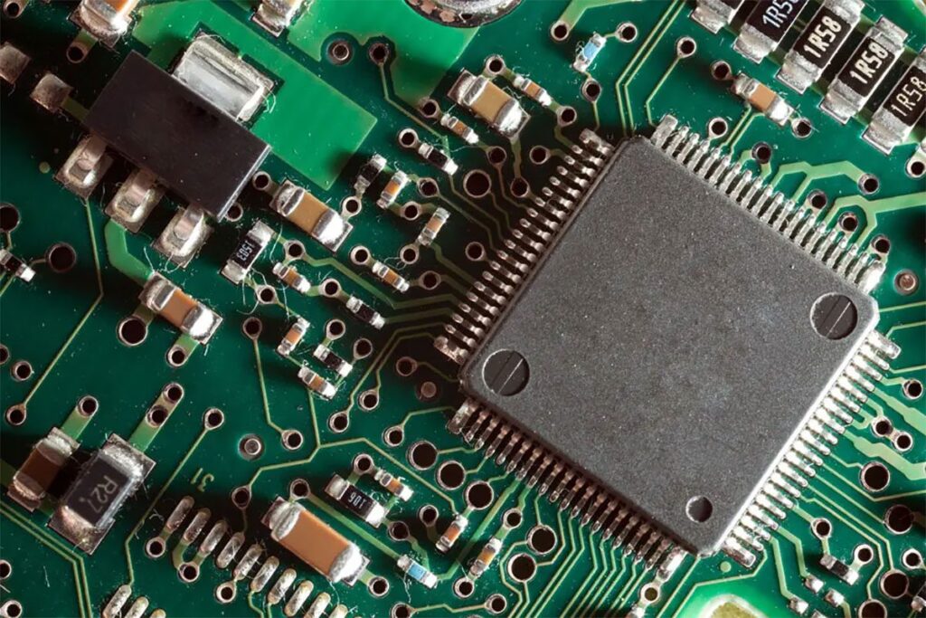
The number of layers does not solely determine the maximum data transfer rate of a 6 layer SSD PCB; several design and material factors influence it. One significant aspect is the quality of the materials used in the PCB’s construction. High-quality dielectric materials can minimize signal loss and improve the overall performance of the PCB. Moreover, the thickness of the copper traces and the layout design directly affect the speed and reliability of data transfer.
The PCB layout design also plays a crucial role in determining the maximum data transfer rate. A well-optimized layout can reduce the length of signal paths and minimize interference from other signals. Differential signalling and impedance matching can enhance signal integrity, allowing faster data transfer rates. Additionally, advanced routing techniques, such as micro vias and blind vias, can improve space utilization and performance, enabling the PCB to handle higher data rates more effectively.
Understand its interface protocol
Interface protocols are vital in determining the maximum data transfer rate achievable by a 6 Layer SSD PCB. The most common interfaces used in modern SSDs are SATA (Serial ATA) and NVMe. While SATA SSDs can deliver data transfer rates of up to 600 MB/s, NVMe SSDs have dramatically higher throughput, with maximum speeds exceeding 3,000 MB/s or more, depending on the configuration and technology.
NVMe takes full advantage of the PCIe (Peripheral Component Interconnect Express) architecture, allowing multiple data lanes to be transmitted simultaneously. This means that a 6 Layer SSD PCB designed with an NVMe interface can leverage the full potential of the high-speed NAND flash memory it houses, resulting in much faster data transfer rates. Users looking for the best performance should consider 6 layer SSD PCBs that utilize NVMe technology, as this combination can significantly enhance overall system performance and responsiveness.
The Role of NAND Flash Memory in Data Transfer Rates
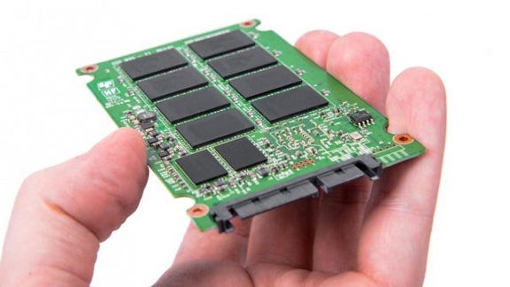
The type of NAND flash memory used in conjunction with a 6-layer SSD PCB is another crucial factor impacting data transfer rates. There are several types of NAND flash memory, including SLC (Single-Level Cell), MLC (Multi-Level Cell), TLC (Triple-Level Cell), and QLC (Quad-Level Cell). Each type offers different performance characteristics, with SLC generally providing the fastest data transfer rates and the best endurance, followed by MLC, TLC, and QLC.
For example, a 6 layer SSD PCB that employs SLC NAND flash can achieve the highest data transfer rates, making it ideal for enterprise applications and tasks that require rapid data access. On the other hand, while TLC and QLC flash memory offer higher storage densities and lower costs, they typically have slower data transfer rates. Therefore, when selecting a 6 layer SSD PCB, users must consider the PCB design and the type of NAND flash memory integrated into the system to achieve optimal performance for their specific needs.
Comparing Data Transfer Rates Across Different SSD Technologies
When considering the maximum data transfer rate of a 6 layer SSD PCBs, it is essential to compare it to other SSD technologies available in the market. For instance, M.2 and U.2 form factors are commonly used in high-performance SSDs, and both can be paired with 6 Layer SSD PCBs to leverage their respective advantages. M.2 SSDs, which connect directly to the motherboard, typically offer faster data transfer rates compared to traditional SATA SSDs, while U.2 SSDs are designed for enterprise storage solutions.
Users should carefully analyze the performance metrics of these SSD technologies to determine which option best meets their requirements. For example, M.2 NVMe SSDs can deliver maximum data transfer rates significantly higher than achievable with a SATA interface. Users seeking high-performance solutions will benefit from understanding these comparisons, as they will inform their decisions when selecting a 6 layer SSD PCB that aligns with their performance goals.
Real-World Applications of 6 Layer SSD PCBs
The impressive data transfer rates achievable with 6 layer SSD PCBs have led to their widespread adoption across various industries and applications. In the gaming industry, for example, the demand for high-speed data access has led to the integration of 6 layer SSDs in gaming consoles and high-performance PCs. The rapid loading times and smooth gameplay of these SSDs offer gamers an unparalleled experience.
Similarly, in video production and editing, professionals rely on 6 layer SSDs to quickly transfer and process large video files. The enhanced data transfer rates allow for real-time editing and playback, significantly improving workflow efficiency. Moreover, in data centers and cloud storage solutions, the ability to handle vast amounts of data with minimal latency makes 6 layer SSD PCBs essential for maintaining optimal performance in these demanding environments.
Future Trends in 6 Layer SSD PCB Technology
As technology advances, we can expect significant innovations in 6 layer SSD PCB design and performance. Future developments include the integration of even faster interface protocols, enhanced thermal management solutions, and improved NAND flash memory technologies. These advancements will likely contribute to even higher maximum data transfer rates, enabling users to achieve unprecedented performance.
Moreover, as the demand for faster and more efficient storage solutions grows, manufacturers will focus on optimizing the design of 6 Layer SSD PCBs to accommodate new technologies and standards. Users can look forward to a future where data transfer rates continue to rise, making 6 layer SSD PCBs an integral component of high-performance computing and storage solutions.
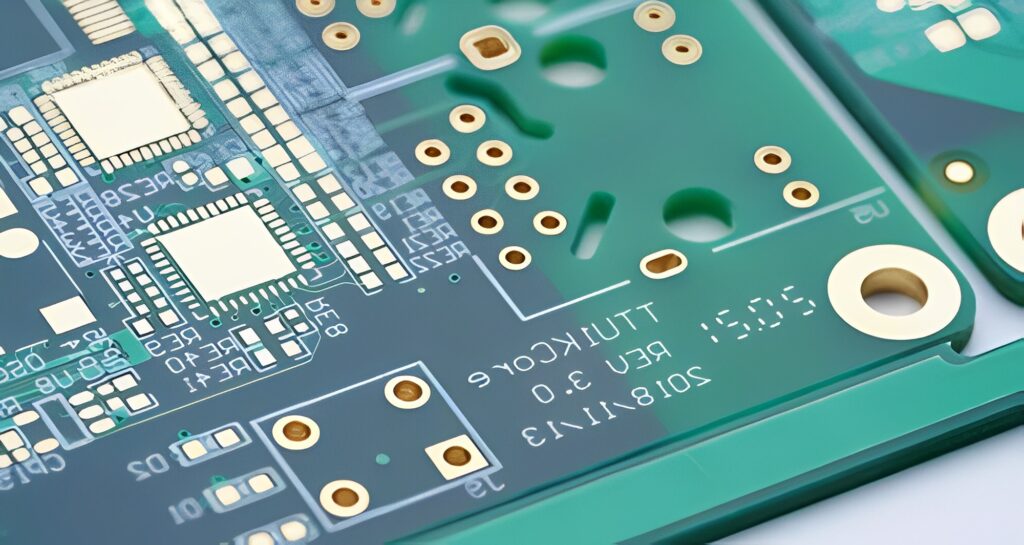
Maximizing Performance with 6 Layer SSD PCB
Various factors, including PCB design, interface protocols, and the type of NAND flash memory used, influence the maximum data transfer rate achievable with a 6 layer SSD PCB. With these elements, users can unlock impressive data transfer rates that cater to demanding applications, from gaming to data-intensive industries.

