
What types of NAND flash memory utilize in 8 layer SSD PCB?
As technology advances, the demand for efficient, high-capacity storage solutions grows. The 8 layer SSD PCB has gained significant attention due to its ability to support increased data storage and maintain high performance. At the heart of these SSD features is the NAND flash memory, which is vital in determining speed, durability, and cost. Next, we will explore the various types of NAND flash memory used in 8 layer SSD PCBs to help potential buyers understand their options and make an informed decision.
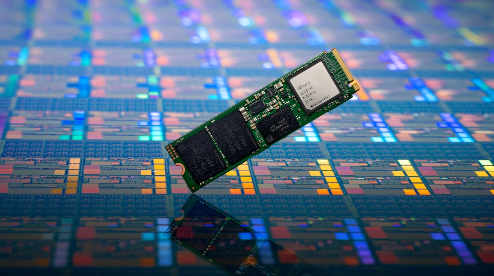
8 Layer SSD PCB The Basics of NAND Flash Memory
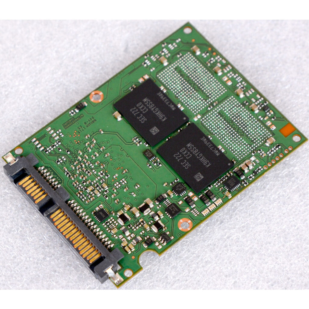
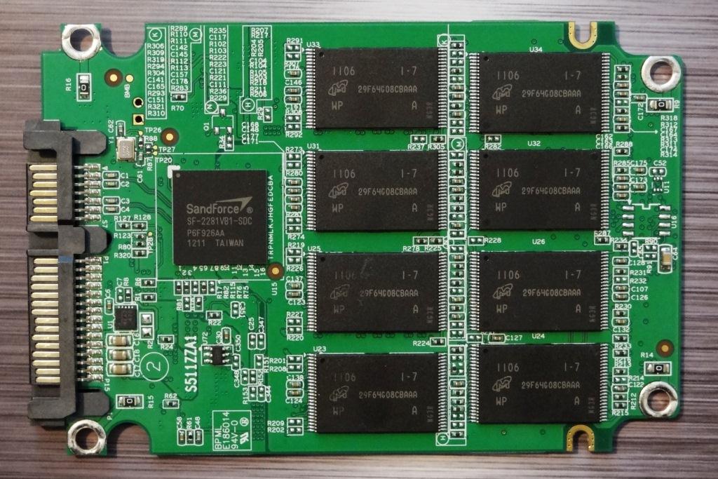
NAND flash memory is a nonvolatile storage technology that retains data even when power is removed. In the context of 8 layer SSD PCBs, NAND flash is the primary component used for data storage. This memory type comes in various forms, each with distinct characteristics influencing performance and cost.
When selecting NAND flash for SSDs, manufacturers typically choose between SLC (Single-Level Cell), MLC (Multi-Level Cell), TLC (Triple-Level Cell), and QLC (Quad-Level Cell). Each type has unique properties, such as storage density, speed, and endurance. Understanding these differences is essential for users seeking the best SSD solution, whether for high-performance applications or more economical options.
Single-Level Cell NAND Flash
Single-level cell (SLC) NAND flash is the most basic type, storing one bit of data per cell. This simplicity translates to high performance and durability, making SLC ideal for enterprise-level applications and high-demand environments. When integrated into an 8 layer SSD PCB, SLC NAND provides rapid read and write speeds and excellent endurance, typically rated at 100,000 program/erase cycles.
While SLC offers superior performance, it is more expensive than other types of NAND flash. This makes it less common in consumer-grade SSDs, which prioritize affordability. However, for applications requiring maximum reliability and speed—such as data centers, financial institutions, and high-performance computing—investing in SLC NAND within an 8 layer SSD PCB is often justified.
Multi-Level Cell NAND Flash
Multi-level cell (MLC) NAND flash stores two bits of data per cell, balancing cost and performance. This type is widely used in consumer SSDs and is suitable for various applications, from gaming to standard office tasks. In 8 layer SSD PCBs, MLC NAND allows for increased storage capacity without significantly sacrificing performance.
MLC NAND flash offers good read and write speeds, but its endurance typically ranges from 3,000 to 10,000 program/erase cycles. This makes it less durable than SLC but more affordable, appealing to users who need a reliable yet cost-effective solution. MLC provides an excellent combination of performance, capacity, and price for most everyday applications, making it a popular choice among consumers.
Triple-Level Cell NAND Flash
Triple-level cell (TLC) NAND flash memory stores three bits of data per cell, further enhancing storage density and reducing costs. TLC is commonly found in consumer-grade SSDs, especially those aimed at budget-conscious users who need large amounts of storage. In the context of 8 layer SSD PCBs, TLC NAND offers significant capacity, which is ideal for mainstream applications.
While TLC NAND is cost-effective, it has limited endurance, typically ranging from 1,000 to 3,000 program/erase cycles. Additionally, write speeds are generally slower than those of SLC and MLC. However, for users whose primary concern is storage capacity—such as those using SSDs for media libraries or general computing—TLC NAND within eight-layer SSD PCBs provides a practical and economical solution.
Quad-Level Cell NAND Flash
Quad-Level Cell (QLC) NAND flash memory takes storage density to the next level by storing four bits of data per cell. This type is particularly appealing for applications requiring maximum capacity at a lower cost, such as cloud storage and large-scale data centres. When integrated into 8 layer SSD PCBs, QLC NAND can provide vast storage while minimizing manufacturing expenses.
However, QLC does come with trade-offs. Its endurance is lower than that of SLC, MLC, and TLC, typically ranging from 100 to 1,000 program/erase cycles. Write speeds can also be slower, especially under heavy workloads. For users who prioritize massive storage without the need for extreme performance—such as in archival or read-intensive scenarios—QLC NAND offers a cost-effective solution.
8 Layer SSD PCB The Role of Controllers and Firmware
While the type of NAND flash memory is crucial, the performance of 8 layer SSD PCBs is also significantly influenced by the SSD controller and firmware. The controller manages data transfer between the NAND flash and the host system, while firmware optimizes read/write operations.
Advanced controllers can improve performance by managing wear levelling, garbage collection, and error correction. For instance, an efficient controller can enhance the endurance of MLC, TLC, and QLC NAND, allowing them to perform closer to SLC levels. When considering 8 layer SSD PCBs, evaluating the overall architecture, including the NAND type and the controller’s capabilities, is essential.
Making Informed Choices for 8 layer SSD PCB
Understanding the type of NAND flash memory used in 8 layer SSD PCBs is critical to making an informed purchasing decision. SLC, MLC, TLC, and QLC each offer unique advantages and limitations for different user needs. By understanding the specific characteristics of these NAND types, users can select the SSD that best suits their performance and capacity requirements.